|
|
|
PDF FAN53541 Data sheet ( Hoja de datos )
| Número de pieza | FAN53541 | |
| Descripción | Synchronous Buck Regulator | |
| Fabricantes | Fairchild Semiconductor | |
| Logotipo | ||
Hay una vista previa y un enlace de descarga de FAN53541 (archivo pdf) en la parte inferior de esta página. Total 15 Páginas | ||
|
No Preview Available !
February 2014
FAN53541
2.4 MHz, 5 A TinyBuck™ Synchronous Buck Regulator
Features
2.4 MHz Fixed-Frequency Operation
Best-in-Class Load Transient Response
5 A Output Current Capability
2.7 V to 5.5 V Input Voltage Range
Adjustable Output Voltage: 0.8 V to 90% of VIN
PFM Mode for High Efficiency in Light Load
(Forced PWM Available on MODE Pin)
50 µA Typical Quiescent Current in PFM Mode
External Frequency Synchronization
Low Ripple Light-Load PFM Mode with Forced
PWM Control
Power Good Output
Internal Soft-Start
Input Under-Voltage Lockout (UVLO)
Thermal Shutdown and Overload Protection
No External Compensation Required
20-Bump WLCSP
Applications
Set-Top Box
Hard Disk Drive
Communications Cards
DSP Power
Description
The FAN53541 is a step-down switching voltage regulator
that delivers an adjustable output from an input voltage
supply of 2.7 V to 5.5 V. Using a proprietary architecture with
synchronous rectification, the FAN53541 is capable of
delivering 5 A at over 90% efficiency, while maintaining a
very high efficiency of over 80% at load currents as low as
2 mA. The regulator operates at a nominal fixed frequency of
2.4 MHz, which reduces the value of the external
components to 470 nH for the output inductor and 20 µF for
the output capacitor. Additional output capacitance can be
added to improve regulation during load transients without
affecting stability and inductance up to 1.2 µH may be used
with additional output capacitance.
At moderate and light loads, pulse frequency modulation
(PFM) is used to operate the device in power-save mode
with a typical quiescent current of 50 µA. Even with such a
low quiescent current, the part exhibits excellent transient
response during large load swings. At higher loads, the
system automatically switches to fixed-frequency control,
operating at 2.4 MHz. In shutdown mode, the supply current
drops below 1 µA, reducing power consumption. PFM mode
can be disabled if constant frequency is desired. The
FAN53541 is available in a 20-bump 1.96 mm x 1.56 mm
Wafer-Level Chip-Scale Package (WLCSP).
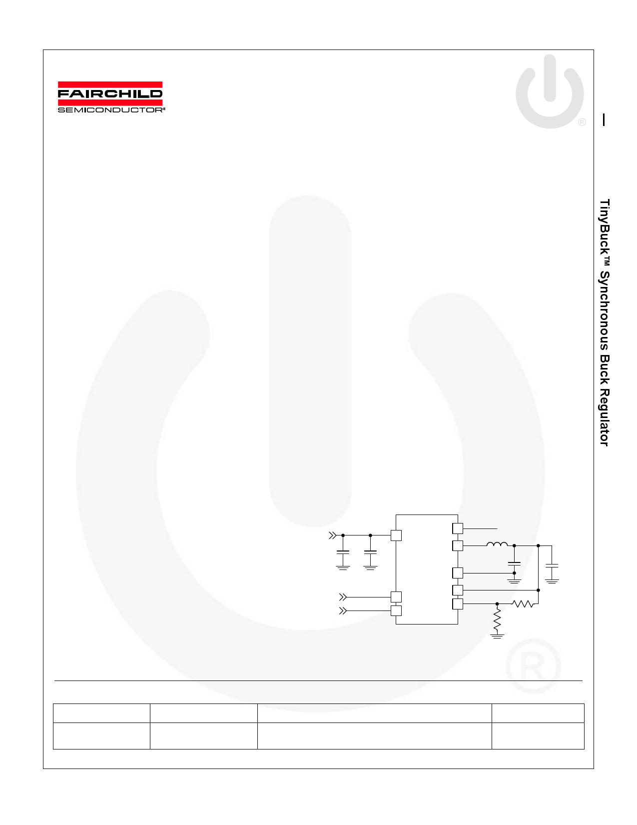
CIN
10µF
VIN
CIN1
10nF
FAN53541
EN
MODE
PGOOD
SW L1
0.47H
GND
COUT
10µF
VOUT
FB
R1
COUT
10µF
Figure 1. Typical Application
Ordering Information
Part Number
FAN53541UCX
Temperature Range
Package
-40 to 85°C
20-Ball Wafer-Level, Chip-Scale Package (WLCSP),
4x5 Array, 0.4 mm Pitch, 250 µm Ball
Packing Method
Tape and Reel
© 2013 Fairchild Semiconductor Corporation
FAN53541 • Rev. 1.0.2
www.fairchildsemi.com
1 page 
Electrical Characteristics
Minimum and maximum values are at VIN=2.7 V to 5.5 V, and TA=-40°C to +85°C, unless otherwise noted. Typical values are
at TA=25°C, VIN=5 V, and VOUT=1.2 V.
Symbol
Power Supplies
Parameter
IQ Quiescent Current
I SD Shutdown Supply Current
VUVLO Under-Voltage Lockout Threshold
VUVHYST Under-Voltage Lockout Hysteresis
Logic Pins
VIH High-Level Input Voltage
VIL Low-Level Input Voltage
VLHYST Logic Input Hysteresis Voltage
IIN Input Bias Current
IOUTL PGOOD Pull-Down Current
IOUTH PGOOD HIGH Leakage Current
VOUT Regulation
VREF
Output Reference DC Accuracy,
Measured at FB Pin
VOUT
ILOAD
Load Regulation
VOUT
VIN
Line Regulation
IREF FB Pin Leakage Current
VOUT Transient Response
Power Switch and Protection
RDS(ON)P P-Channel MOSFET On Resistance
RDS(ON)N N-Channel MOSFET On Resistance
ILIMPK P-MOS Peak Current Limit
TLIMIT Thermal Shutdown
THYST Thermal Shutdown Hysteresis
VSDWN Input OVP Shutdown
Frequency Control
fSW Oscillator Frequency
fMODE MODE Pin Synchronization Range
Soft-Start and Output Discharge
tSS
Regulator Enable to Regulated VOUT
(Rising PGOOD)
RDIS Output Discharge Resistance
Condition
Min. Typ. Max. Unit
ILOAD=0, MODE=0 (AUTO PFM/PWM)
ILOAD=0, MODE=1 (Forced PWM)
EN=GND
VIN Rising
VIN Falling
50 µA
30 mA
0.1 10 µA
2.67 2.80 V
2.1 2.3
V
365 mV
Input Tied to GND or 1 kΩ Resistor to VIN
VPGOOD=0.4 V
VPGOOD=VIN
1.05
1
140
0.01
0.01
V
0.4 V
mV
1.00 µA
mA
1.00 µA
TA=25°C, Forced PWM
TA=-40°C to 85°C, Forced PWM
AUTO PFM/PWM
MODE=VIN (Forced PWM)
0.792
0.787
0.784
0.800
0.800
0.800
0.808
0.813
0.824
V
V
V
–0.02
%/A
2.7 V ≤ VIN ≤ 5.5 V, IOUT(DC)=1.5 A
FB=0.8 V
ILOAD Step 0.1 A to 1.5 A, tR=100 ns
-0.16
1
-30
%/V
nA
mV
Open Loop
Closed Loop
Rising Threshold
Falling Threshold
33 mΩ
28 mΩ
5.8 7.5 8.8 A
8A
155 °C
20 °C
6.1 V
5.5 5.8
V
External Square-Wave, 30% to 70% Duty
Cycle
2.1 2.4 3.0 MHz
525 600 700 kHz
EN=0 V
1.2 ms
175 Ω
© 2013 Fairchild Semiconductor Corporation
FAN53541 • Rev. 1.0.2
5
www.fairchildsemi.com
5 Page 
PGOOD Pin
The PGOOD pin is an open-drain that indicates that the IC is
in regulation when its state is open. PGOOD pulls LOW
under the following conditions:
The IC has operated in cycle-by-cycle current limit for
eight consecutive PWM cycles;
The circuit is disabled, either after a fault occurs or when
EN is LOW; or
The IC is performing a soft-start.
Thermal Shutdown
When the die temperature increases, due to a high load
condition and/or a high ambient temperature, the output
switching is disabled until the temperature on the die has
fallen sufficiently. The junction temperature at which the
thermal shutdown activates is nominally 155°C with a
20°C hysteresis.
Minimum Off-Time Effect on Switching
Frequency
tOFF(MIN) is 45 ns, which constrains the maximum VOUT/VIN
that the FAN53541 can provide, while still maintaining a fixed
switching frequency in PWM Mode. Regulation is maintained
even though the regulator is unable to provide sufficient
duty-cycle and operate at 2.4 MHz.
Switching frequency is the lower of 2.4 MHz or:
fSW (MHz) 22.2 1
VOUT IOUT ROFF
VIN IOUT (ROFF RON )
(4)
where:
IOUT = load current, in A;
RON = RDS(ON)_P + DCRL, in Ohms; and
ROFF = RDS(ON)_N + DCRL, in Ohms.
A result of <0 MHz indicates 100% duty cycle operation.
Application Information
Selecting the Inductor
The output inductor must meet both the required inductance
and the energy handling capability of the application. The
inductor value affects the average current limit, output
voltage ripple, transient response, and efficiency.
The ripple current (∆I) of the regulator is:
I
VOUT
VIN
VIN
L
VOUT
fSW
(5)
The maximum average load current, IMAX(LOAD), is related to
the peak current limit, ILIM(PK), by the ripple current as:
IMAX(LOAD)
ILIM(PK)
I
2
(6)
The FAN53541 is optimized for operation with L=470 nH, but
is stable with inductances up to 1.2 H (nominal). The
inductor should be rated to maintain at least 80% of its value
at ILIM(PK). Failure to do so lowers the amount of DC current
the IC can deliver.
Efficiency is affected by the inductor DCR and inductance
value. Decreasing the inductor value for a given physical
size typically decreases the DCR; but since ∆I increases, the
RMS current increases, as do core and skin-effect losses.
IRMS
IOUT(DC)2
I2
12
(7)
The increased RMS current produces higher losses through
the RDS(ON) of the IC MOSFETs as well as the inductor ESR.
Increasing the inductor value produces lower RMS currents,
but degrades transient response. For a given physical
inductor size, increased inductance usually results in an
inductor with lower saturation current.
Table 3 shows the effects on regulator performance of higher
inductance than the recommended 470 nH.
Table 3. Inductor Value and Regulator
Performance
IMAX(LOAD)
Increase
∆VOUT (Eq.(8))
Decrease
Transient Response
Degraded
Inductor Current Rating
The FAN53541’s current-limit circuit can allow a peak current
of about 8.8 A to flow through L1 under worst-case
conditions. If it is possible for the load to draw that much
continuous current, the inductor should be capable of
sustaining that current or failing in a safe manner.
For space-constrained applications, a lower current rating for
L1 can be used. The FAN53541 may still protect these
inductors in the event of a short circuit, but may not be able
to protect the inductor from failure if the load is able to draw
higher currents than the DC rating of the inductor.
© 2013 Fairchild Semiconductor Corporation
FAN53541 • Rev. 1.0.2
11
www.fairchildsemi.com
11 Page | ||
| Páginas | Total 15 Páginas | |
| PDF Descargar | [ Datasheet FAN53541.PDF ] | |
Hoja de datos destacado
| Número de pieza | Descripción | Fabricantes |
| FAN53541 | Synchronous Buck Regulator | Fairchild Semiconductor |
| Número de pieza | Descripción | Fabricantes |
| SLA6805M | High Voltage 3 phase Motor Driver IC. |
Sanken |
| SDC1742 | 12- and 14-Bit Hybrid Synchro / Resolver-to-Digital Converters. |
Analog Devices |
|
DataSheet.es es una pagina web que funciona como un repositorio de manuales o hoja de datos de muchos de los productos más populares, |
| DataSheet.es | 2020 | Privacy Policy | Contacto | Buscar |