|
|
|
PDF NTLJF1103P Data sheet ( Hoja de datos )
| Número de pieza | NTLJF1103P | |
| Descripción | Power MOSFET and Schottky Diode | |
| Fabricantes | ON Semiconductor | |
| Logotipo | ||
Hay una vista previa y un enlace de descarga de NTLJF1103P (archivo pdf) en la parte inferior de esta página. Total 4 Páginas | ||
|
No Preview Available !
NTLJF1103P
Product Preview
Power MOSFET and
Schottky Diode
−8 V, −4.3 A, mCool] P−Channel, with
2.0 A Schottky Barrier Diode, 2x2 mm,
WDFN Package
Features
• WDFN 2x2 mm Package with Exposed Drain Pad for
Excellent Thermal Conduction
• Footprint Same as SC−88 Package
• 1.5 V VGS Rated RDS(on)
• Low VF, 2 A Schottky Diode
• Low Profile (< 0.8 mm) for Easy Fit in Thin Environment
• This is a Pb−Free Device
Applications
• DC−DC Buck Converter
• Low Voltage Hard Disk DC Power Source
MOSFET MAXIMUM RATINGS (TJ = 25°C unless otherwise noted)
Parameter
Symbol Value Unit
Drain−to−Source Voltage
Gate−to−Source Voltage
Continuous Drain Current
(Note 1)
Power Dissipation
(Note 1)
Continuous Drain Current
(Note 2)
Power Dissipation
(Note 2)
Steady
State
t≤5s
Steady
State
t≤5s
Steady
State
TA = 25°C
TA = 85°C
TA = 25°C
TA = 25°C
TA = 25°C
TA = 85°C
TA = 25°C
VDSS
VGS
ID
PD
ID
PD
−8
±6
−3.5
−2.5
−4.3
1.5
2.3
−2.4
−1.7
0.7
V
V
A
W
A
W
Pulsed Drain Current
tp = 10 ms
Operating Junction and Storage Temperature
Source Current (Body Diode)
Single Pulse Drain−to−Source Avalanche Energy
(VDD = V, VG = V, IPK = A, RG = W)
IDM
TJ,
TSTG
IS
EAS
−17
−55 to
150
−1.9
TBD
A
°C
A
mJ
Lead Temperature for Soldering Purposes
(1/8″ from case for 10 s)
TL 260 °C
Stresses exceeding Maximum Ratings may damage the device. Maximum
Ratings are stress ratings only. Functional operation above the Recommended
Operating Conditions is not implied. Extended exposure to stresses above the
Recommended Operating Conditions may affect device reliability.
1. Surface Mounted on FR4 Board using 2 in sq pad size
(Cu area = 1.127 in sq [2 oz] including traces).
2. Surface Mounted on FR4 Board using the minimum recommended pad size.
This document contains information on a product under development. ON Semiconductor
reserves the right to change or discontinue this product without notice.
© Semiconductor Components Industries, LLC, 2006
April, 2006 − Rev. P0
1
http://onsemi.com
V(BR)DSS
−8 V
MOSFET
RDS(on) Max
90 mW @ −4.5 V
120 mW @ −2.5 V
150 mW @ −1.8 V
170 mW @ −1.5 V
ID Max (Note 1)
−4.3 A
SCHOTTKY DIODE
VR Max
20 V
VF Typ
0.37 V
IF Max
2.0 A
DA
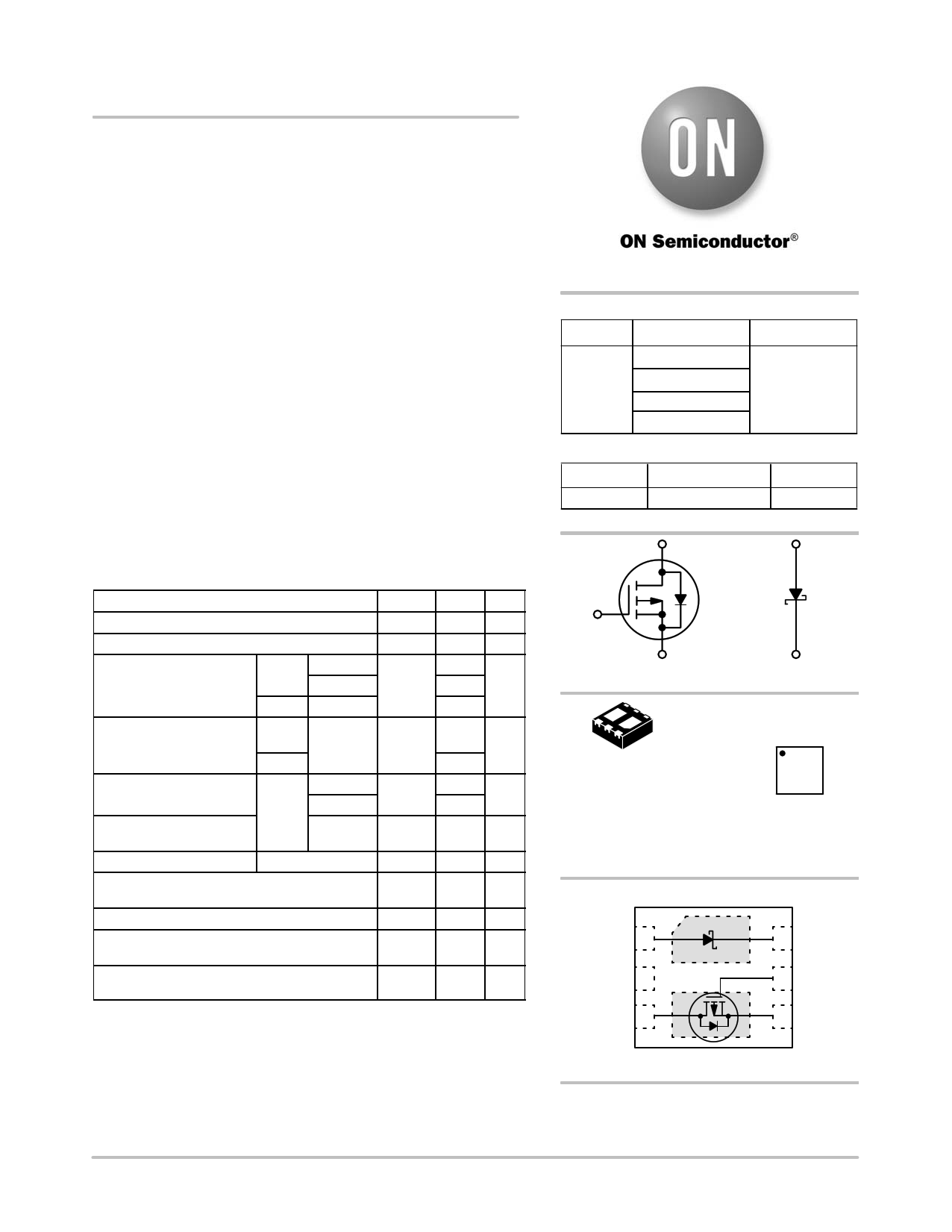
G
S
P−CHANNEL MOSFET
K
SCHOTTKY DIODE
1
WDFN6
CASE 506AN
MARKING
DIAGRAM
16
2 JG M G 5
3 G4
JG = Specific Device Code
M = Date Code
G = Pb−Free Package
(Note: Microdot may be in either location)
PIN CONNECTIONS
A1
K
6K
N/C 2
D3
5G
D
4S
(Top View)
ORDERING INFORMATION
See detailed ordering and shipping information in the package
dimensions section on page 3 of this data sheet.
Publication Order Number:
NTLJF1103P/D
1 page | ||
| Páginas | Total 4 Páginas | |
| PDF Descargar | [ Datasheet NTLJF1103P.PDF ] | |
Hoja de datos destacado
| Número de pieza | Descripción | Fabricantes |
| NTLJF1103P | Power MOSFET and Schottky Diode | ON Semiconductor |
| Número de pieza | Descripción | Fabricantes |
| SLA6805M | High Voltage 3 phase Motor Driver IC. |
Sanken |
| SDC1742 | 12- and 14-Bit Hybrid Synchro / Resolver-to-Digital Converters. |
Analog Devices |
|
DataSheet.es es una pagina web que funciona como un repositorio de manuales o hoja de datos de muchos de los productos más populares, |
| DataSheet.es | 2020 | Privacy Policy | Contacto | Buscar |