|
|
|
PDF 2N3055AG Data sheet ( Hoja de datos )
| Número de pieza | 2N3055AG | |
| Descripción | Complementary Silicon High-Power Transistors | |
| Fabricantes | ON Semiconductor | |
| Logotipo | ||
Hay una vista previa y un enlace de descarga de 2N3055AG (archivo pdf) en la parte inferior de esta página. Total 6 Páginas | ||
|
No Preview Available !
2N3055AG (NPN),
MJ15015G (NPN),
MJ15016G (PNP)
Complementary Silicon
High-Power Transistors
These PowerBase complementary transistors are designed for high
power audio, stepping motor and other linear applications. These
devices can also be used in power switching circuits such as relay or
solenoid drivers, dc−to−dc converters, inverters, or for inductive loads
requiring higher safe operating area than the 2N3055.
Features
• High Current−Gain − Bandwidth
• Safe Operating Area
• These Devices are Pb−Free and are RoHS Compliant*
MAXIMUM RATINGS (Note 1)
Rating
Symbol
Value
Unit
Collector−Emitter Voltage
2N3055AG
MJ15015G, MJ15016G
VCEO
60
120
Vdc
Collector−Base Voltage
2N3055AG
MJ15015G, MJ15016G
VCBO
100
200
Vdc
Collector−Emitter Voltage Base
Reversed Biased
2N3055AG
MJ15015G, MJ15016G
VCEV
100
200
Vdc
Emitter−Base Voltage
Collector Current − Continuous
Base Current
Total Device Dissipation
@ TC = 25_C
2N3055AG
MJ15015G, MJ15016G
Derate above 25_C
2N3055AG
MJ15015G, MJ15016G
VEBO
IC
IB
PD
7.0
15
7.0
115
180
Vdc
Adc
Adc
W
W
0.65 W/_C
1.03 W/_C
Operating and Storage Junction
Temperature Range
TJ, Tstg −65 to +200
_C
Stresses exceeding Maximum Ratings may damage the device. Maximum
Ratings are stress ratings only. Functional operation above the Recommended
Operating Conditions is not implied. Extended exposure to stresses above the
Recommended Operating Conditions may affect device reliability.
1. Indicates JEDEC Registered Data. (2N3055A)
THERMAL CHARACTERISTICS
Characteristics
Thermal Resistance, Junction−to−Case
Symbol
RqJC
Max Max Unit
1.52 0.98 _C/W
*For additional information on our Pb−Free strategy and soldering details, please
download the ON Semiconductor Soldering and Mounting Techniques
Reference Manual, SOLDERRM/D.
© Semiconductor Components Industries, LLC, 2013
September, 2013 − Rev. 7
1
http://onsemi.com
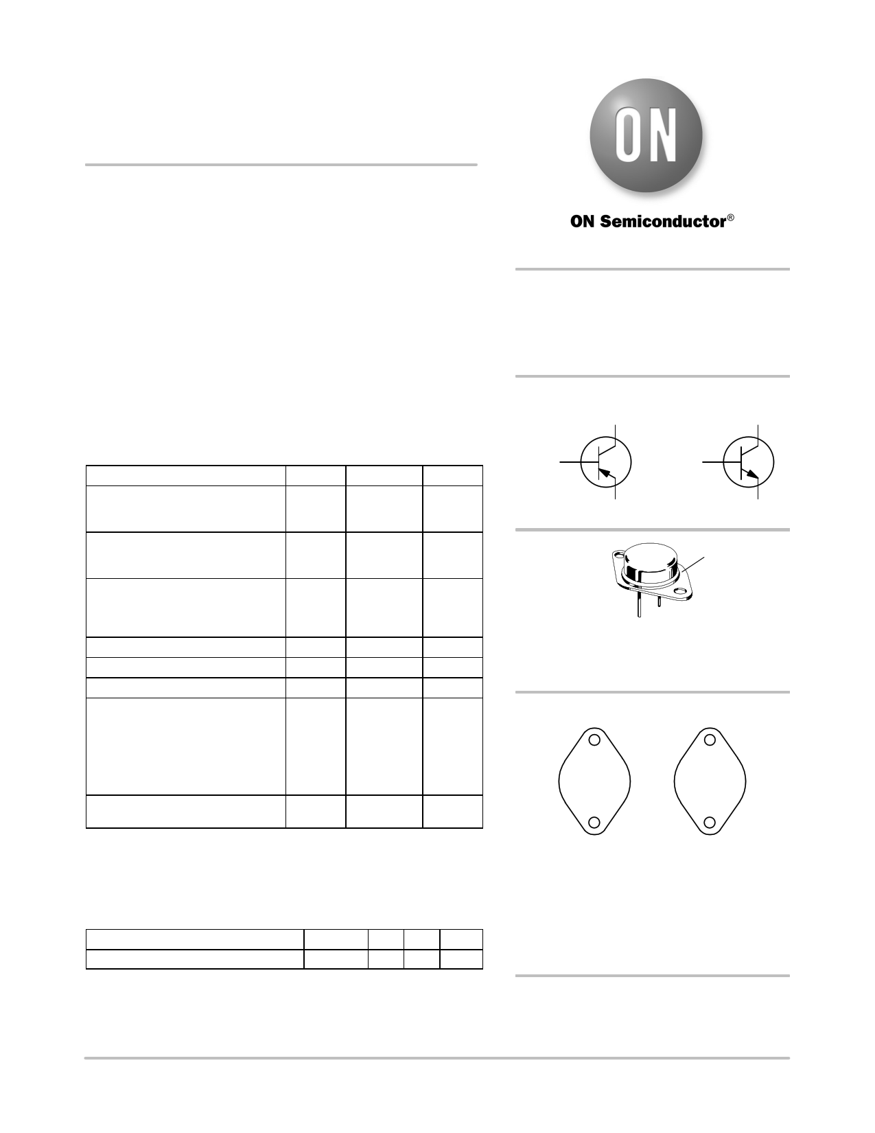
15 AMPERE
COMPLEMENTARY SILICON
POWER TRANSISTORS
60, 120 VOLTS − 115, 180 WATTS
PNP
CASE 3
NPN
CASE 3
BASE
1
BASE
1
EMITTER 2
EMITTER 2
CASE
2
1
TO−204 (TO−3)
CASE 1−07
STYLE 1
MARKING DIAGRAMS
2N3055AG
AYWW
MEX
MJ1501xG
AYWW
MEX
2N3055A = Device Code
MJ1501x = Device Code
x = 5 or 6
G = Pb−Free Package
A = Assembly Location
Y = Year
WW = Work Week
MEX
= Country of Origin
ORDERING INFORMATION
See detailed ordering and shipping information in the package
dimensions section on page 5 of this data sheet.
Publication Order Number:
2N3055A/D
1 page 
2N3055AG (NPN), MJ15015G (NPN), MJ15016G (PNP)
NPN
10,000
1000
VCE = 30 V
COLLECTOR CUT−OFF REGION
PNP
1000
VCE = 30 V
100
100
TJ = 150°C
10
100°C
1.0
0.1 REVERSE
IC = ICES
FORWARD
0.01
+ 0.2
25°C
+ 0.1 0 - 0.1 - 0.2 - 0.3 - 0.4
VBE, BASE-EMITTER VOLTAGE (VOLTS)
Figure 10. 2N3055A, MJ15015
- 0.5
20
30 ms
10
100 ms
1 ms
5
BONDING WIRE LIMIT
2 THERMAL LIMIT @ TC = 25°C
(SINGLE PULSE)
SECOND BREAKDOWN LIMIT
100 ms
dc
1
10 20
60 100
VCE, COLLECTOR-EMITTER VOLTAGE (VOLTS)
Figure 12. Forward Bias Safe Operating Area
2N3055A
10 TJ = 150°C
1.0
100°C
0.1
REVERSE
0.01 25°C
IC = ICES
FORWARD
0.001
- 0.2
20
10
- 0.1 0 + 0.1 + 0.2 + 0.3 + 0.4
VBE, BASE-EMITTER VOLTAGE (VOLTS)
Figure 11. MJ15016
+ 0.5
0.1 ms
5.0
1.0 ms
2.0
1.0
0.5
0.2
15
BONDING WIRE LIMIT
THERMAL LIMIT @ TC = 25°C
(SINGLE PULSE)
SECOND BREAKDOWN LIMIT
100 ms
dc
20 30
60 100
VCE, COLLECTOR-EMITTER VOLTAGE (VOLTS)
120
Figure 13. Forward Bias Safe Operating Area
MJ15015, MJ15016
There are two limitations on the power handling ability of
a transistor: average junction temperature and second
breakdown. Safe Operating area curves indicate IC − VCE
limits of the transistor that must be observed for reliable
operation; i.e., the transistor must not be subjected to greater
dissipation than the curves indicate.
The data of Figures 12 and 13 is based on TC = 25_C;
TJ(pk) is variable depending on power level. Second
breakdown pulse limits are valid for duty cycles to 10% but
must be derated for temperature according to Figure 1.
ORDERING INFORMATION
Device
2N3055AG
MJ15015G
MJ15016G
Package
TO−204
(Pb−Free)
TO−204
(Pb−Free)
TO−204
(Pb−Free)
http://onsemi.com
5
Shipping
100 Units / Tray
100 Units / Tray
100 Units / Tray
5 Page | ||
| Páginas | Total 6 Páginas | |
| PDF Descargar | [ Datasheet 2N3055AG.PDF ] | |
Hoja de datos destacado
| Número de pieza | Descripción | Fabricantes |
| 2N3055A | POWER TRANSISTORS(15A) | Mospec Semiconductor |
| 2N3055A | 15 AMPERE COMPLEMENTARY SILICON POWER TRANSISTORS 60/ 120 VOLTS 115/ 180 WATTS | Motorola Inc |
| 2N3055A | COMPLEMENTARY SILICON POWER TRANSISTORS | ON Semiconductor |
| 2N3055A | COMPLEMENTARY SILICON HIGH-POWER TRANSISTORS | Boca Semiconductor Corporation |
| Número de pieza | Descripción | Fabricantes |
| SLA6805M | High Voltage 3 phase Motor Driver IC. |
Sanken |
| SDC1742 | 12- and 14-Bit Hybrid Synchro / Resolver-to-Digital Converters. |
Analog Devices |
|
DataSheet.es es una pagina web que funciona como un repositorio de manuales o hoja de datos de muchos de los productos más populares, |
| DataSheet.es | 2020 | Privacy Policy | Contacto | Buscar |