|
|
|
PDF HCPL-315J Data sheet ( Hoja de datos )
| Número de pieza | HCPL-315J | |
| Descripción | 0.5 Amp Output Current IGBT Gate Drive Optocoupler | |
| Fabricantes | Avago | |
| Logotipo | ||
Hay una vista previa y un enlace de descarga de HCPL-315J (archivo pdf) en la parte inferior de esta página. Total 21 Páginas | ||
|
No Preview Available !
HCPL-3150 (Single Channel), HCPL-315J (Dual Channel)
0.5 Amp Output Current IGBT Gate Drive Optocoupler
Data Sheet
Lead (Pb) Free
RoHS 6 fully
compliant
RoHS 6 fully compliant options available;
-xxxE denotes a lead-free product
Description
The HCPL-315X consists of an LED optically coupled
to an integrated circuit with a power output stage. This
optocoupler is ideally suited for driving power IGBTs and
MOSFETs used in motor control inverter applications.
The high operating voltage range of the output stage
provides the drive voltages required by gate controlled
devices. The voltage and current supplied by this opto-
coupler makes it ideally suited for directly driving IGBTs
with ratings up to 1200 V/50 A. For IGBTs with higher rat-
ings, the HCPL-3150/315J can be used to drive a discrete
power stage which drives the IGBT gate.
Applications
• Isolated IGBT/MOSFET gate drive
• AC and brushless dc motor drives
• Industrial inverters
• Switch Mode Power Supplies (SMPS)
• Uninterruptable Power Supplies (UPS)
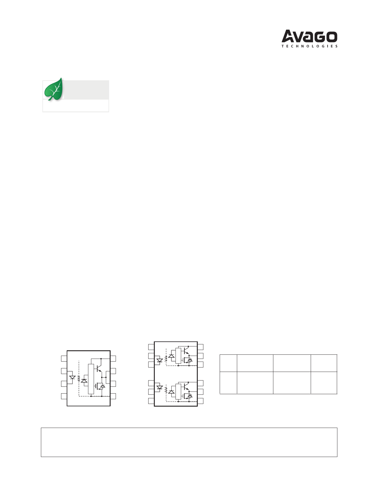
Functional Diagram
Features
• 0.6A maximum peak output current
• 0.5 A minimum peak output current
• 15 kV/µs minimum Common Mode Rejection (CMR)
at VCM = 1500 V
•
1.0 V maximum low
eliminates need for
level output voltage
negative gate drive
(
VOL)
• ICC = 5 mA maximum supply current
• Under Voltage Lock-Out protection (UVLO) with
hysteresis
• Wide operating VCC range: 15 to 30 volts
• 0.5 µs maximum propagation delay
• +/– 0.35 µs maximum delay between devices/
channels
• Industrial temperature range: -40°C to 100°C
• HCPL-315J: channel one to channel two output
isolation = 1500 Vrms/1 min.
• Safety and regulatory approval:
UL recognized (UL1577),
3750 Vrms/1 min (HCPL-3150)
5000 Vrms/1 min (HCPL-315J)
IEC/EN/DIN EN 60747-5-5 approved
VIORM
VIORM
=
=
6134014VVpepaeka(kH(HCCPPL-L3-311550Jo)pCtSioAnc0e6rt0ifioendly)
N/C 1
ANODE 2
CATHODE 3
N/C 4
SHIELD
HCPL-3150
N/C 1
8 VCC
ANODE 2
CATHODE 3
7 VO
6 VO
ANODE 6
CATHODE 7
5 VEE
N/C 8
SHIELD
SHIELD
HCPL-315J
16 VCC
15 VO
14 VEE
11 VCC
10 VO
9 VEE
TRUTH TABLE
L ED LE D POSVI“TCP(ICiVo.e–Es.i-VV,tGCiETCvOEu-eIrVNnGEGET-o ORinnUg)T N”H EGTAVABCT“LCINV(E–ieE.Vge-G.Ea,VEOtCTiCIvuN-erVGn-EG-EOofinf)g ” VO
O FFOOFNF (i.e.0T-U3R000NV---O31N01)VV
(i.e. 0TU- R30N-V00O-F-9F3.)05VV
LOW
VO
LOW
LOW
ONON 0 - 1111 V- 13.5 V
0 - 9.59V.5 - 12 V LOW TRANSITION
ONON 11 - 1133..55V- 30 V 9.5 - 121V2 - 30 V TRANSITION HIGH
ON 13.5 - 30 V
12 - 30 V
HIGH
A 0.1 µF bypass capacitor must be connected between the VCC and VEE pins for each channel.
CAUTION: It is advised that normal static precautions be taken in handling and assembly of this
component to prevent damage and/or degradation which may be induced by ESD. The components
featured in this datasheet are not to be used in military or aerospace applications or environments.
1 page 
Recommended Pb-Free IR Profile
Recommended reflow condition as per JEDEC Standard, J-STD-020 (latest revision). Non-Halide Flux should be used.
Regulatory Information
The HCPL-3150 and HCPL-315J have been approved by the following organizations:
UL Recognized under UL 1577, Component Recognition Program, File E55361.
CSA Approved under CSA Component Acceptance Notice #5, File CA 88324.
IEC/EN/DIN EN 60747-5-5 Approved under: DIN EN 60747-5-5(VDE 0884-5):2011-11 (Option 060 and HCPL-315J only)
IEC/EN/DIN EN 60747-5-5 Insulation Characteristics
Description
Installation classification per DIN VDE 0110/1.89, Table 1
for rated mains voltage ≤ 150 Vrms
for rated mains voltage ≤ 300 Vrms
for rated mains voltage ≤ 600 Vrms
for rated mains voltage ≤ 1000Vrms
Climatic Classification
Pollution Degree (DIN VDE 0110/1.89)
Maximum Working Insulation Voltage
Input to Output Test Voltage, Method b*
VPIaOrRMtiaxl1d.i8s7c5ha=rgVePR<, 1500p%C Production Test with tm = 1 sec,
Input to Output Test Voltage, Method a*
VPIaOrRMtiaxl
1d.6isc=hVaPrRg, Tey<pe5
and
pC
Sample
Test,
tm
=
10
sec,
Highest Allowable Overvoltage*
(Transient Overvoltage tini = 60 sec)
Safety-Limiting Values – Maximum Values Allowed in the
Event of a Failure, Also See Figure 37, Thermal Derating Curve.
Case Temperature
Input Current
Output Power
Insulation Resistance at TS, VIO = 500 V
Symbol
VIORM
VPR
VPR
VIOTM
TS
IS, INPUT
PS, OUTPUT
RS
HCPL-3150#060 HCPL-315J
I - IV
I - III
I - II
55/100/21
2
630
I - IV
I - IV
I - IV
I-III
55/100/21
2
1414
1181
2652
Unit
Vpeak
Vpeak
945
6000
2262
8000
Vpeak
Vpeak
175
230
600
≥ 109
175
400
1200
≥ 109
°C
mA
mW
Ω
* Refer to IEC/EN/DIN EN 60747-5-5 Optoisolator Safety Standard section of the Avago Regulatory Guide to Isolation Circuits, AV02-2041EN for a
detailed description of Method a and Method b partial discharge test profiles.
Note: Isolation characteristics are guaranteed only within the safety maximum ratings which must be ensured by protective circuits in application.
5
5 Page 
500
IF = 10 mA
TA = 25 °C
Rg = 47 Ω
400 Cg = 3 nF
DUTY CYCLE = 50%
f = 10 kHz
300
TPLH
TPHL
500
VCC = 30 V, VEE = 0 V
Rg = 47 Ω, Cg = 3 nF
400
TA = 25 °C
DUTY CYCLE = 50%
f = 10 kHz
300
500
IF(ON) = 10 mA
IF(OFF) = 0 mA
400
VCC = 30 V, VEE = 0 V
Rg = 47 Ω, Cg = 3 nF
DUTY CYCLE = 50%
f = 10 kHz
300
200
100 15
20
25
VCC – SUPPLY VOLTAGE – V
Figure 10. Propagation Delay vs. VCC.
30
200
TPLH
TPHL
100 6 8 10 12 14 16
IF – FORWARD LED CURRENT – mA
Figure 11. Propagation Delay vs. IF.
200
TPLH
TPHL
100-40 -20 0 20 40 60 80 100
TA – TEMPERATURE – °C
Figure 12. Propagation Delay vs. Temperature.
500
VCC = 30 V, VEE = 0 V
TA = 25 °C
400
IF = 10 mA
Cg = 3 nF
DUTY CYCLE = 50%
f = 10 kHz
300
500
VCC = 30 V, VEE = 0 V
TA = 25 °C
400
IF = 10 mA
Rg = 47 Ω
DUTY CYCLE = 50%
f = 10 kHz
300
200
TPLH
TPHL
100
0
50 100 150 200
Rg – SERIES LOAD RESISTANCE – Ω
Figure 13. Propagation Delay vs. Rg.
200
TPLH
TPHL
100
0 20 40 60 80 100
Cg – LOAD CAPACITANCE – nF
Figure 14. Propagation Delay vs. Cg.
30
25
20
15
10
5
0
01 2 3 4 5
IF – FORWARD LED CURRENT – mA
Figure 15. Transfer Characteristics.
1000
100
10
1.0
IF
VF+–
TA = 25°C
0.1
0.01
0.0011.10 1.20 1.30 1.40 1.50 1.60
VF – FORWARD VOLTAGE – V
Figure 16. Input Current vs. Forward Voltage.
11
11 Page | ||
| Páginas | Total 21 Páginas | |
| PDF Descargar | [ Datasheet HCPL-315J.PDF ] | |
Hoja de datos destacado
| Número de pieza | Descripción | Fabricantes |
| HCPL-3150 | 0.5 Amp Output Current IGBT Gate Drive Optocoupler | Agilent(Hewlett-Packard) |
| HCPL-3150 | 0.5 Amp Output Current IGBT Gate Drive Optocoupler | Avago |
| HCPL-315J | 0.5 Amp Output Current IGBT Gate Drive Optocoupler | Agilent |
| HCPL-315J | 0.5 Amp Output Current IGBT Gate Drive Optocoupler | Avago |
| Número de pieza | Descripción | Fabricantes |
| SLA6805M | High Voltage 3 phase Motor Driver IC. |
Sanken |
| SDC1742 | 12- and 14-Bit Hybrid Synchro / Resolver-to-Digital Converters. |
Analog Devices |
|
DataSheet.es es una pagina web que funciona como un repositorio de manuales o hoja de datos de muchos de los productos más populares, |
| DataSheet.es | 2020 | Privacy Policy | Contacto | Buscar |