|
|
|
PDF CS8361 Data sheet ( Hoja de datos )
| Número de pieza | CS8361 | |
| Descripción | 5.0V Dual Micropower Low Dropout Regulator | |
| Fabricantes | ON Semiconductor | |
| Logotipo | ||
Hay una vista previa y un enlace de descarga de CS8361 (archivo pdf) en la parte inferior de esta página. Total 8 Páginas | ||
|
No Preview Available !
CS8361
5.0 V Dual Micropower
Low Dropout Regulator
with ENABLE and RESET
The CS8361 is a precision Micropower dual voltage regulator with
ENABLE and RESET.
The 5.0 V standby output is accurate within ±2% while supplying
loads of 100 mA and has a typical dropout voltage of 400 mV.
Quiescent current is low, typically 140 mA with a 300 mA load. The
active RESET output monitors the 5.0 V standby output and is low
during power−up and regulator dropout conditions. The RESET
circuit includes hysteresis and is guaranteed to operate correctly with
1.0 V on the standby output.
The second output tracks the 5.0 V standby output through an
external adjust lead, and can supply loads of 250 mA with a typical
dropout voltage of 400 mV. The logic level ENABLE lead is used to
control this tracking regulator output.
Both outputs are protected against overvoltage, short circuit, reverse
battery and overtemperature conditions. The robustness and low
quiescent current of the CS8361 makes it not only well suited for
automotive microprocessor applications, but for any battery powered
microprocessor applications.
Features
• 2 Regulated Outputs
− Standby Output 5.0 V ± 2%; 100 mA
− Tracking Output 5.0 V; 250 mA
• Low Dropout Voltage (0.4 V at Rated Current)
• RESET Option
• ENABLE Option
• Low Quiescent Current
• Protection Features
− Independent Thermal Shutdown
− Short Circuit
− 60 V Load Dump
− Reverse Battery
• Internally Fused Leads in SO−16L Package
• These are Pb−Free Devices
http://onsemi.com
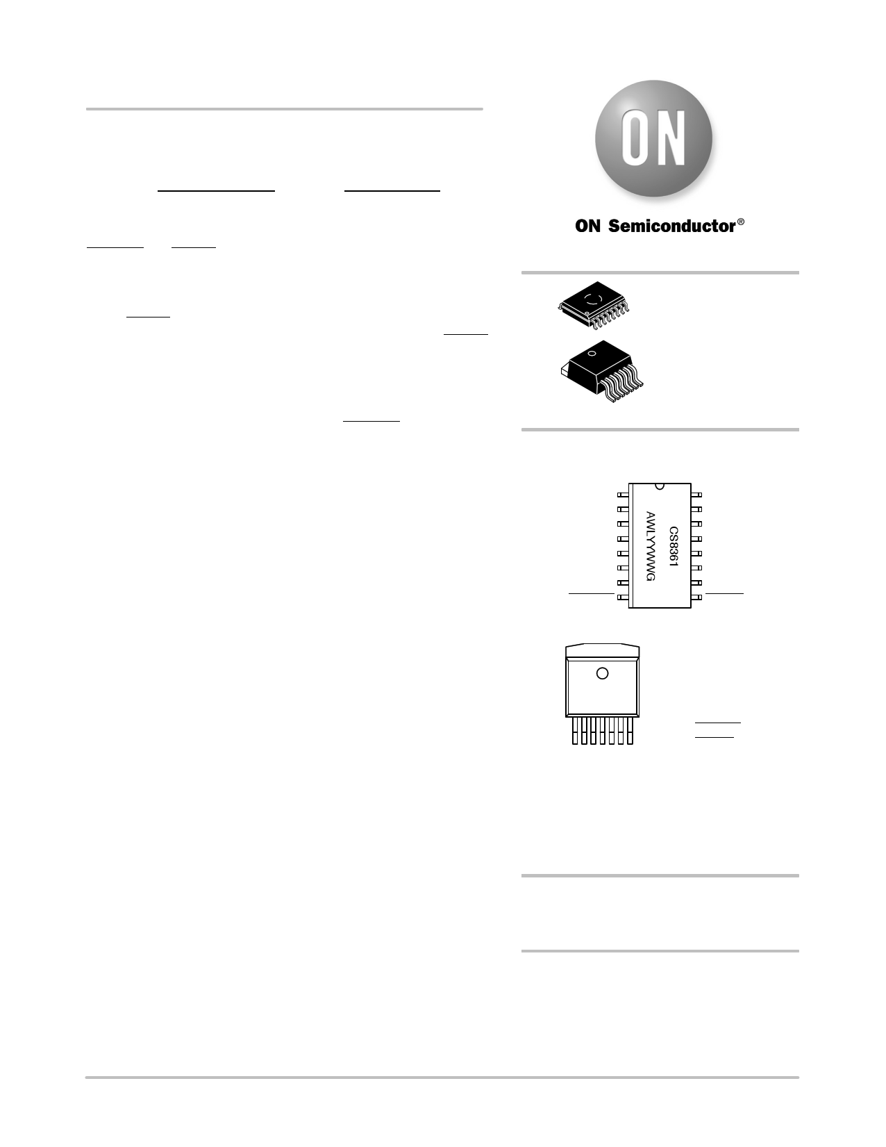
SO−16L
DW SUFFIX
CASE 751G
D2PAK−7
DPS SUFFIX
CASE 936AB
1
PIN CONNECTIONS AND
MARKING DIAGRAM
1
VIN
NC
VTRK
GND
GND
Adj
NC
ENABLE
16
VSTBY
NC
NC
GND
GND
NC
NC
RESET
SO−16L
CS
8361
AWLYWWG
1
Pin 1. VSTBY
2. VIN
3. VTRK
4. GND
5. Adj
6. ENABLE
7. RESET
D2PAK−7
CS8361 = Device Code
A = Assembly Location
WL = Wafer Lot
YY = Year
WW = Work Week
G = Pb−Free Package
ORDERING INFORMATION
See detailed ordering and shipping information in the package
dimensions section on page 6 of this data sheet.
*For additional information on our Pb−Free strategy
and soldering details, please download the
ON Semiconductor Soldering and Mounting
Techniques Reference Manual, SOLDERRM/D.
© Semiconductor Components Industries, LLC, 2009
October, 2009 − Rev. 17
1
Publication Order Number:
CS8361/D
1 page 
CS8361
5.0 V, 100 mA
B+
C1* VIN
VSTBY
C2**
VDD
0.1 mF
CS8361
R3 10 mF
MCU
RESET
ESR < 8.0 W
RESET
ENABLE
I/O
Adj
GND
VTRK
SW 5.0 V,
C3**
250 mA
10 mF
ESR < 8.0 W
GND
*C1 is required if regulator is located far from power supply filter.
**C2 and C3 are required for stability.
Figure 3. Test and Application Circuit, Dual 5.0 V Regulator
APPLICATION NOTES
External Capacitors
Output capacitors for the CS8361 are required for
stability. Without them, the regulator outputs will oscillate.
Actual size and type may vary depending upon the
application load and temperature range. Capacitor effective
series resistance (ESR) is also a factor in the IC stability.
Worst−case is determined at the minimum ambient
temperature and maximum load expected.
Output capacitors can be increased in size to any desired
value above the minimum. One possible purpose of this
would be to maintain the output voltages during brief
conditions of negative input transients that might be
characteristic of a particular system.
Capacitors must also be rated at all ambient temperatures
expected in the system. To maintain regulator stability down
to −40°C, capacitors rated at that temperature must be used.
More information on capacitor selection for SMART
REGULATOR®s is available in the SMART REGULATOR
application note, “Compensation for Linear Regulators,”
document number SR003AN/D, available through the
Literature Distribution Center or via our website at
http://www.onsemi.com.
Calculating Power Dissipation in a
Dual Output Linear Regulator
The maximum power dissipation for a dual output
regulator (Figure 4) is
PD(max) + NJVIN(max) * VOUT1(min)NjIOUT1(max) )
NJVIN(max) * VOUT2(min)NjIOUT2(max) ) VIN(max)IQ (1)
where:
VIN(max) is the maximum input voltage,
VOUT1(min) is the minimum output voltage from VOUT1,
VOUT2(min) is the minimum output voltage from VOUT2,
IOUT1(max) is the maximum output current, for the
application,
IOUT2(max) is the maximum output current, for the
application, and
IQ is the quiescent current the regulator consumes at both
IOUT1(max) and IOUT2(max).
Once the value of PD(max) is known, the maximum
permissible value of RqJA can be calculated:
RQJA
+
150°
C*
PD
TA
(2)
The value of RqJA can be compared with those in the
package section of the data sheet. Those packages with
RqJA’s less than the calculated value in equation 2 will keep
the die temperature below 150°C.
In some cases, none of the packages will be sufficient to
dissipate the heat generated by the IC, and an external
heatsink will be required.
IIN
VIN
SMART
REGULATOR
IOUT1
VOUT1
Control
Features
IOUT2
VOUT2
IQ
Figure 4. Dual Output Regulator With Key
Performance Parameters Labeled.
http://onsemi.com
5
5 Page | ||
| Páginas | Total 8 Páginas | |
| PDF Descargar | [ Datasheet CS8361.PDF ] | |
Hoja de datos destacado
| Número de pieza | Descripción | Fabricantes |
| CS8361 | 5V Dual Micropower Low Dropout Regulator with ENABLE and RESET | Cherry Semiconductor Corporation |
| CS8361 | 5.0V Dual Micropower Low Dropout Regulator | ON Semiconductor |
| CS8361YDPS7 | 5V Dual Micropower Low Dropout Regulator with ENABLE and RESET | Cherry Semiconductor Corporation |
| CS8361YDPSR7 | 5V Dual Micropower Low Dropout Regulator with ENABLE and RESET | Cherry Semiconductor Corporation |
| Número de pieza | Descripción | Fabricantes |
| SLA6805M | High Voltage 3 phase Motor Driver IC. |
Sanken |
| SDC1742 | 12- and 14-Bit Hybrid Synchro / Resolver-to-Digital Converters. |
Analog Devices |
|
DataSheet.es es una pagina web que funciona como un repositorio de manuales o hoja de datos de muchos de los productos más populares, |
| DataSheet.es | 2020 | Privacy Policy | Contacto | Buscar |