|
|
PDF MR25H10 Data sheet ( Hoja de datos )
| Número de pieza | MR25H10 | |
| Descripción | 1Mb Serial SPI MRAM | |
| Fabricantes | Everspin Technologies | |
| Logotipo |  |
|
Hay una vista previa y un enlace de descarga de MR25H10 (archivo pdf) en la parte inferior de esta página. Total 20 Páginas | ||
|
No Preview Available !
FEATURES
• No write delays
• Unlimited write endurance
• Data retention greater than 20 years
• Automatic data protection on power loss
• Block write protection
• Fast, simple SPI interface with up to 40 MHz clock rate
• 2.7 to 3.6 Volt power supply range
• Low current sleep mode
• Industrial temperatures
• Available in 8-pin DFN or 8-pin DFN Small Flag RoHS-compliant
packages
• Direct replacement for serial EEPROM, Flash, FeRAM
• AEC-Q100 Grade 1 Option
MR25H10
1Mb Serial SPI MRAM
DFN
Small Flag DFN
INTRODUCTION
The MR25H10 is a 1,048,576-bit magnetoresistive random access memory
(MRAM) device organized as 131,072 words of 8 bits. The MR25H10 offers serial
EEPROM and serial Flash compatible read/write timing with no write delays and
unlimited read/write endurance.
RoHS
Unlike other serial memories, both reads and writes can occur randomly in memory with no delay between
writes. The MR25H10 is the ideal memory solution for applications that must store and retrieve data and
programs quickly using a small number of I/O pins.
The MR25H10 is available in either a 5 mm x 6 mm 8-pin DFN package or a 5 mm x 6 mm 8-pin DFN Small
Flag package. Both are compatible with serial EEPROM, Flash, and FeRAM products.
The MR25H10 provides highly reliable data storage over a wide range of temperatures. The product is
offered with Industrial (-40° to +85 °C) and AEC-Q100 Grade 1 (-40°C to +125 °C) operating temperature
range options.
CONTENTS
1. DEVICE PIN ASSIGNMENT......................................................................... 2
2. SPI COMMUNICATIONS PROTOCOL...................................................... 4
3. ELECTRICAL SPECIFICATIONS................................................................. 10
4. TIMING SPECIFICATIONS.......................................................................... 12
5. ORDERING INFORMATION....................................................................... 12
6. MECHANICAL DRAWING.......................................................................... 13
7. REVISION HISTORY...................................................................................... 15
How to Reach Us.......................................................................................... 15
Copyright © Everspin Technologies 2015
1
MR25H10 Rev. 9.2, 6/2015
1 page 
MR25H10
SPI COMMUNICATIONS PROTOCOL
Table 2.3 Block Memory Write Protection
Status Register
BP1 BP0
00
01
10
11
Protected Area
None
Upper Quarter
Upper Half
All
Memory Contents
Unprotected Area
All Memory
Lower Three-Quarters
Lower Half
None
WEL
0
1
1
1
SRWD
X
0
1
1
WP
X
X
Low
High
Table 2.4 Memory Protection Modes
Protected Blocks
Protected
Protected
Protected
Protected
Unprotected Blocks
Protected
Writable
Writable
Writable
Status
Register
Protected
Writable
Protected
Writable
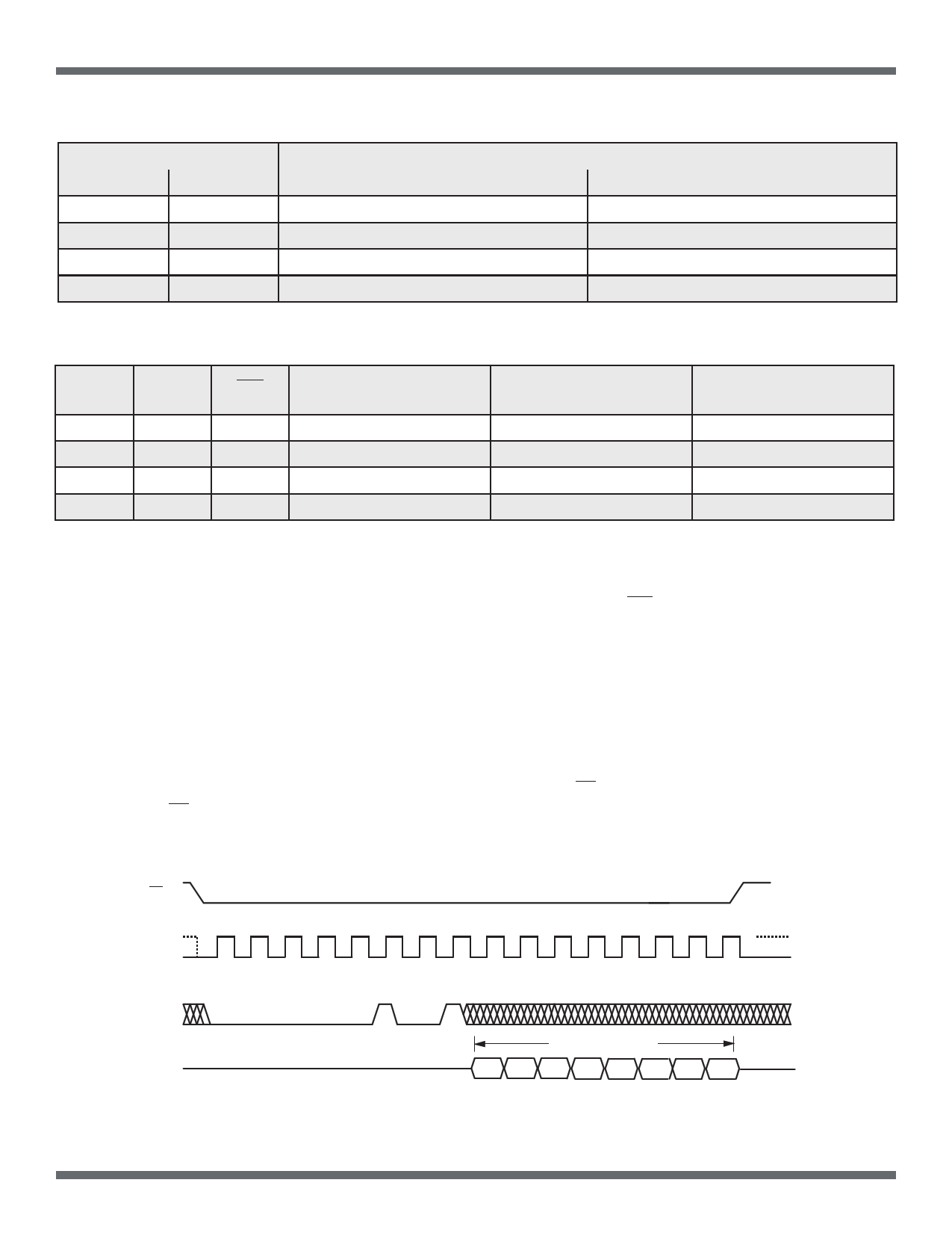
When WEL is reset to 0, writes to all blocks and the status register are protected. When WEL is set to 1,
BP0 and BP1 determine which memory blocks are protected. While SRWD is reset to 0 and WEL is set to 1,
status register bits BP0 and BP1 can be modified. Once SRWD is set to 1, WP must be high to modify SRWD,
BP0 and BP1.
Read Status Register (RDSR)
The Read Status Register (RDSR) command allows the Status Register to be read. The Status Register can
be read at any time to check the status of write enable latch bit, status register write protect bit, and block
write protect bits. For MR25H10, the write in progress bit (bit 0) is not written by the memory because
there is no write delay. The RDSR command is entered by driving CS low, sending the command code, and
then driving CS high.
Figure 2.1 RDSR
CS
SCK
0 1 2 3 4 5 6 7 0 1 2 3 4 5 6 7 Mode 3
Mode 0
SI 0 0 0 0 0 1 0 1
MSB
Status Register Out
SO High Impedance
7 6 5 4 3 2 1 0 High Z
MSB
Copyright © Everspin Technologies 2015
5
MR25H10 Rev. 9.2, 6/2015
5 Page 
MR25H10
ELECTRICAL SPECIFICATIONS
Table 3.2 Operating Conditions
Symbol Parameter
VDD Power supply voltage
Grade
Industrial
AEC-Q100 Grade1
Min Max Unit
2.7 3.6
V
3.0 3.6
V
VIH Input high voltage
All
2.2 VDD + 0.3
V
VIL Input low voltage
All
-0.5 0.8
V
Industrial
TA
Temperature under bias
AEC-Q100 Grade1 1
-40 85
-40 125
°C
°C
1 AEC-Q100 Grade 1 temperature profile assumes 10 percent duty cycle at maximum temperature (2 years
out of 20-year life.)
Table 3.3 DC Characteristics
Symbol
ILI
ILO
VOL
VOH
Parameter
Input leakage current
Conditions
Output leakage current
Output low voltage
Output high voltage
IOL = +4 mA
IOL = +100 μA
(IOH = -4 mA)
(IOH = -100 μA)
Min
-
-
-
-
2.4
VDD - 0.2
Typical
-
-
-
-
-
-
Max
±1
±1
0.4
VSS + 0.2v
-
-
Unit
μA
μA
V
V
V
V
Table 3.4 Power Supply Characteristics
Symbol Parameter
IDDR Active Read Current
IDDW Active Write Current
Conditions
1 MHz
40 MHz
1 MHz
40 MHz
Typical Max Unit
2.5 3 mA
6 10 mA
8 13 mA
23 27 mA
ISB Standby Current
CS high and SPI bus inactive
90
115 μA
Izz Standby Sleep Mode Current CS high and SPI bus inactive
7
30 μA
Copyright © Everspin Technologies 2015
11
MR25H10 Rev. 9.2, 6/2015
11 Page | ||
| Páginas | Total 20 Páginas | |
| PDF Descargar | [ Datasheet MR25H10.PDF ] | |
Hoja de datos destacado
| Número de pieza | Descripción | Fabricantes |
| MR25H10 | 1Mb Serial SPI MRAM | Everspin Technologies |
| Número de pieza | Descripción | Fabricantes |
| SLA6805M | High Voltage 3 phase Motor Driver IC. |
Sanken |
| SDC1742 | 12- and 14-Bit Hybrid Synchro / Resolver-to-Digital Converters. |
Analog Devices |
|
DataSheet.es es una pagina web que funciona como un repositorio de manuales o hoja de datos de muchos de los productos más populares, |
| DataSheet.es | 2020 | Privacy Policy | Contacto | Buscar |
