|
|
|
PDF AR7100 Data sheet ( Hoja de datos )
| Número de pieza | AR7100 | |
| Descripción | High Performance And Cost-Effective Network Processor | |
| Fabricantes | Atheros | |
| Logotipo | ||
Hay una vista previa y un enlace de descarga de AR7100 (archivo pdf) en la parte inferior de esta página. Total 30 Páginas | ||
|
No Preview Available !
Data Sheet
December 2008
AR7100: A Scalable, High Performance And Cost-Effective
Network Processor Family
General Description
Features
The Atheros AR7100 is a scalable, high
performance and cost effective network
processor family that allows efficient design of
solutions addressing triple play services such
as voice, video and data for home and
enterprise access point, router and gateway
applications. It includes a 32-bit MIPS
processor, PCI host interface, two 802.3
Ethernet MACs with GMII/RGMII/RMII/MII
interface, two USB 2.0 MAC/PHYs, a PCM
interface for glueless SLIC support, external
memory interface for serial Flash and DDR-
SDRAM, a high-speed UART, I2S interface, and
GPIOs that can be used for LED controls.
The AR7100 network processor when paired
with the AR9100 chipset family (AR9160
MAC/baseband processor and AR9106/
AR9104/AR9103/AR9102/AR9101 radios)
provides the best in class WLAN solution
capable of supporting 802.11a/b/g/n
standards.
■ Integrated MIPS 24K-family processor
■ 300–680 MHz processor frequency:
– AR7130, 300 MHz, Fast Ethernet version
– AR7141, 400 MHz, supports Fast
Ethernet and GB Ethernet
– AR7161, 680 MHz, supports Fast
Ethernet and GB Ethernet
■ High Performance DDR memory controller
(16- or 32-bit)
■ Dual IEEE 802.3 Ethernet MAC supporting
10/100/1000 Mbps, full and half duplex
and GMII/RGMII/RMII/MII interfaces
■ Two-port USB 2.0 Host Controllers with
built-in MAC/PHY
■ UART for console support
■ 32-bit, 33/66 MHz PCI 2.3 host interface
supporting up to three client devices
■ IEEE 1149.1 standard test access port and
boundary scan architecture supported
■ JTAG based debugging of the processor
core supported
■ 13 mm x 13 mm 384 TFBGA lead-free
package
■ Along with the Atheros AR9100 (MAC/BB
and radio chips) family—Completes an all-
CMOS solution for 802.11a/b/g/n WLANs,
supporting extended range for worldwide
operations
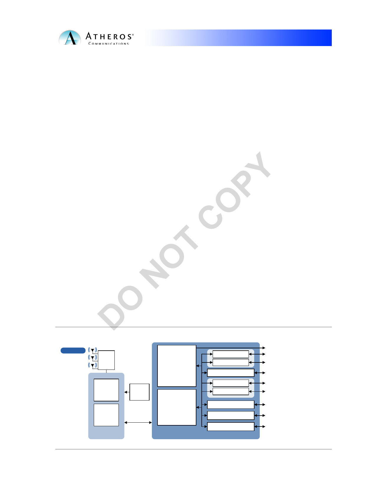
System Block Diagram
2.4/5 GHz
3x
FEM
DDR Controller
and Memory
Interface
AR9103/
AR9106
AR9160
AR9100
40
MHz
Crystal
PCI
Interface
MIPS Processor
AR7100
Ethernet MAC
Ethernet MAC
High Speed UART
USB MAC/PHY
USB MAC/PHY
External Interface
PCM Interface
I2S
Serial Flash/DDR Interface
RGMII Interface
RGMII Interface
UART Interface
USB 2.0 Interface
USB 2.0 Interface
GPIOs/LEDs
SLIC
Audio Interface
© 2000-2008 by Atheros Communications, Inc. All rights reserved. Atheros®, Atheros Driven®, Atheros XR®, Driving the Wireless Future®, ROCm®, Super
AG®, Super G®, Total 802.11n®, and Wake on Wireless® are registered by Atheros Communications, Inc. Atheros SST™, Signal-Sustain Technology™, the Air
is Cleaner at 5-GHz™, XSPAN™, Wireless Future. Unleashed Now.™, and 5-UP™ are trademarks of Atheros Communications, Inc. The Atheros logo is a
registered trademark of Atheros Communications, Inc. All other trademarks are the property of their respective holders. Subject to change without notice.
COMPANY CONFIDENTIAL
•1
1 page 
5.8.7 PCI Interrupt Status
(RST_PCI_INTERRUPT_STATUS)
71
5.8.8 PCI Interrupt Mask
(RST_PCI_INTERRUPT_MASK) 71
5.8.9 Global Interrupt Status
(RST_GLOBAL_INTERRUPT_STA
TUS) .............................................. 71
5.8.10 Reset (RST_RESET) ..................... 72
5.8.11 Performance Counter Control
(PERF_CONTROL) ..................... 73
5.8.12 Performance Counter 0
(PERF0_COUNTER) ................... 74
5.8.13 Performance Counter 1
(PERF1_COUNTER) ................... 74
5.8.14 Chip Revision ID
(RST_REVISION_ID) ................. 74
5.9 MII Registers ........................................... 75
5.9.1 MII0 Control (MII0_CNTL) ....... 75
5.9.2 MII1 Control (MII1_CNTL) ....... 75
5.10 SLIC Registers ....................................... 76
5.10.1 SLIC Status (SLIC_STATUS_REG)
76
5.10.2 SLIC Control (SLIC_CNTRL_REG)
76
5.10.3 Time Slice Assigned to Slot 0
(SLIC_SLOT0_NUM) ................. 77
5.10.4 Time Slice Assigned to Slot 1
(SLIC_SLOT1_NUM) ................. 77
5.10.5 SLIC Sample Position
(SLIC_SAM_POS) ....................... 77
5.10.6 SLIC Frequency Divider
(SLIC_FREQ_DIVIDER) ............ 77
5.11 SLIC/I2S DMA Registers ..................... 78
5.11.1 DMA Base Address for SLIC Slot 0
Rx Channel (DMA_0_ADDRESS)
78
5.11.2 Configure DMA SLIC Slot 0 Rx
Channel (DMA_0_CONFIG) ..... 79
5.11.3 Buffer Queueing for SLIC Slot 0 Rx
Channel (DMA_0_UPDATE) .... 79
5.11.4 DMA Base Address for SLIC Slot 1
Rx Channel (DMA_1_ADDRESS)
79
5.11.5 Configure DMA SLIC Slot 1 Rx
Channel (DMA_1_CONFIG) ..... 80
5.11.6 Buffer Queueing for SLIC Slot 1 Rx
Channel (DMA_1_UPDATE) .... 80
5.11.7 DMA Base Address for the Stereo-
to-Rx Channel
(DMA_2_ADDRESS) .................. 80
5.11.8 Configure DMA Stereo-to-Rx
Channel (DMA_2_CONFIG) .... 81
5.11.9 Buffer Queueing for the Stereo-to-
Rx Channel (DMA_2_UPDATE) 81
5.11.10 DMA Base Address for the SLIC
Device 0 Tx Channel
(DMA_3_ADDRESS) .................. 82
5.11.11 Configure DMA for the SLIC
Device 0 Tx channel
(DMA_3_CONFIG) .................... 82
5.11.12 Buffer Queueing for the SLIC
Device 0 Tx Channel
(DMA_3_UPDATE) .................... 83
5.11.13 DMA Base Address for the SLIC
Device 1 Tx Channel
(DMA_4_ADDRESS) .................. 83
5.11.14 Configure DMA for the SLIC
Device 1 Tx Channel
(DMA_4_CONFIG) .................... 83
5.11.15 Buffer Queueing for the SLIC
Device 1 Tx Channel
(DMA_4_UPDATE) .................... 84
5.11.16 DMA Base Address for the Stereo
Tx Channel (DMA_5_ADDRESS)
84
5.11.17 Configure DMA for the Stereo Tx
Channel (DMA_5_CONFIG) .... 84
5.11.18 Buffer Queueing for the Stereo Tx
Channel (DMA_5_UPDATE) .... 85
5.11.19 DMA Interrupt (DMA_INT) ... 85
5.12 Stereo Registers ..................................... 86
5.12.1 Configure the Stereo Block
(STEREO_CONFIG) ................... 86
5.12.2 Set the Stereo Volume
(STEREO_VOLUME) ................. 88
5.13 Ethernet Registers ................................. 89
5.13.1 MAC Configuration 1 ................ 90
5.13.2 MAC Configuration 2 ................ 91
5.13.3 IPG/IFG ....................................... 91
5.13.4 Half-Duplex ................................. 92
5.13.5 Maximum Frame Length ........... 92
5.13.6 MII Configuration ...................... 93
5.13.7 MII Command ............................ 93
Atheros Communications, Inc.
COMPANY CONFIDENTIAL
AR7100 Network Processor Family • 5
December 2008 • 5
5 Page 
Table 1-5 and Table 1-6 provide the signal-to-
pin relationship information for the AR7100.
Table 1-5. Signal-to-Pin Relationships
Pull-Up/
Signal Name Pin Direction Pull-Down Voltage Description
Reset and Reference Clock
COLD_RST_L A13
SYS_RST_L A16
REF_CLK
R24
I
O
I
None
None
None
3.3 V
3.3 V
3.3 V
Reset entire chip
System reset for external devices
40 MHz reference clock
GPIO
GPIO_0[1]
GPIO_1[1]
GPIO_2[1]
GPIO_3[1]
GPIO_4[1]
GPIO_5[1]
GPIO_6[1]
GPIO_7[1]
GPIO_8[1]
GPIO_9[1]
GPIO_10[1]
GPIO_11[1]
C20
B21
A23
B20
A22
A21
A20
A19
B19
C19
A18
B18
I/O
I/O
I/O
I/O
I/O
I/O
I/O
I/O
I/O
I/O
I/O
I/O
None
None
None
None
None
None
None
None
None
None
None
None
3.3 V
3.3 V
3.3 V
3.3 V
3.3 V
3.3 V
3.3 V
3.3 V
3.3 V
3.3 V
3.3 V
3.3 V
General purpose I/O pins, 8 mA drive strength
I2S
I2S_SCK[1]
I2S_SDI[1]
I2S_SDO[1]
I2S_WS[1]
B19
B18
A20
A19
O
I
O
O
None
None
None
None
3.3 V
3.3 V
3.3 V
3.3 V
Clock
Serial audio data in
Serial audio data out
Word select for stereo
0 Right
1 Left
JTAG Interface
JTAG_ENABLE
TDI
TDO
TMS
TCK
TRST_L
B13
B17
A17
C17
C18
B16
I
I
O
I
I
I
None
None
None
None
None
None
3.3 V
3.3 V
3.3 V
3.3 V
3.3 V
3.3 V
JTAG interface enable
JTAG data input
JTAG data output
JTAG mode select
JTAG Clock
JTAG reset
PCM
DRA[1] A23 O
DXA[1] B20 I
FS[1]
A21 O
PCLK[1] A22 O
None
None
None
None
3.3 V
3.3 V
3.3 V
3.3 V
Data transmitted from the AR7100 to the SLIC
Data transmitted from the SLIC to the AR7100
Frame sync
Clock
Atheros Communications, Inc.
COMPANY CONFIDENTIAL
AR7100 Network Processor Family • 11
December 2008 • 11
11 Page | ||
| Páginas | Total 30 Páginas | |
| PDF Descargar | [ Datasheet AR7100.PDF ] | |
Hoja de datos destacado
| Número de pieza | Descripción | Fabricantes |
| AR7100 | High Performance And Cost-Effective Network Processor | Atheros |
| Número de pieza | Descripción | Fabricantes |
| SLA6805M | High Voltage 3 phase Motor Driver IC. |
Sanken |
| SDC1742 | 12- and 14-Bit Hybrid Synchro / Resolver-to-Digital Converters. |
Analog Devices |
|
DataSheet.es es una pagina web que funciona como un repositorio de manuales o hoja de datos de muchos de los productos más populares, |
| DataSheet.es | 2020 | Privacy Policy | Contacto | Buscar |