|
|
PDF SST11CP15 Data sheet ( Hoja de datos )
| Número de pieza | SST11CP15 | |
| Descripción | 4.9-5.8 GHz High-Linearity Power Amplifier | |
| Fabricantes | Silicon Storage Technology | |
| Logotipo | ||
Hay una vista previa y un enlace de descarga de SST11CP15 (archivo pdf) en la parte inferior de esta página. Total 11 Páginas | ||
|
No Preview Available !
4.9-5.8 GHz High-Linearity Power Amplifier
SST11CP15
FEATURES:
• Small Package Size
• High Linear Output Power:
– 802.11a OFDM Spectrum mask compliance up
to 23 dBm
– Added EVM~2.5% up to 18 dBm, typically,
across 5.1-5.8 GHz for 54 Mbps 802.11a signal
• High Power-added Efficiency/Low Operating
Current for 54 Mbps 802.11a Applications
– ~11% @ POUT = 19 dBm for 54 Mbps
• Gain:
– Typically 26 dB gain across broadband
4.9-5.8 GHz
• Low Idle Current
– ~120 mA ICQ
• High Speed Power-up/-down
– Turn on/off time (10%~90%) <100 ns
• Low Shut-down Current (<1 µA)
• On-chip Power Detection
• 20 dB Dynamic Range On-chip Power Detection
• 50Ω On-chip Input Matching and Simple Output
Matching
• Packages Available
– 12-contact UQFN (2mm x 2mm x 0.6mm max
thickness)
APPLICATIONS:
• WLAN (IEEE 802.11a/n)
• Japan WLAN
• HyperLAN2
• Multimedia
Data Sheet
PRODUCT DESCRIPTION
The SST11CP15 is a high-linearity power amplifier that has
low power consumption and is based on the highly-reliable
InGaP/GaAs HBT technology.
The SST11CP15 can be easily configured for high-linearity,
high-efficiency applications with superb power-added effi-
ciency while operating over the entire 802.11a frequency
band for U.S., European, and Japanese markets (4.9-5.8
GHz).
The SST11CP15 has excellent linearity, typically ~2.5%
added EVM at 18 dBm output power which is essential for
54 Mbps 802.11a operation while meeting 802.11a spec-
trum mask at 23 dBm. SST11CP15 also has wide-range,
single-ended power detectors which lower users’ cost on
power control.
The power amplifier IC also features easy board-level
usage along with high-speed power-up/down control. Low
reference current (total IREF <5 mA) makes the
SST11CP15 controllable by an on/off switching signal
directly from the baseband chip. These features coupled
with low operating current make the SST11CP15 ideal for
the final stage power amplification in battery-powered
802.11a WLAN transmitter and access point applications.
The SST11CP15 is offered in 12-contact UQFN package
with 0.6 mm maximum thickness. See Figure 2 for pin
assignments and Table 1 for pin descriptions.
©2011 Silicon Storage Technology, Inc.
S71428-01-000
01/11
1
The SST logo and SuperFlash are registered Trademarks of Silicon Storage Technology, Inc.
These specifications are subject to change without notice.
1 page 
4.9-5.8 GHz High-Linearity Power Amplifier
SST11CP15
TYPICAL PERFORMANCE CHARACTERISTICS
Test Conditions: VCC = 3.3V, TA = 25°C, VREG = 2.85V unless otherwise noted
EVM for 54 Mbps Operation
Data Sheet
EVM versus Output Power
10
9
8 Freq=4.9 GHz
7 Freq=5.1 GHz
Freq=5.5 GHz
6 Freq=5.825 GHz
5
4
3
2
1
0
0 1 2 3 4 5 6 7 8 9 10 11 12 13 14 15 16 17 18 19 20 21
Output Power (dBm)
1428 F4.1
FIGURE 3: EVM versus Output Power
Supply Current versus Output Power
300
290
280
270
260
250
240
230
220
210
200
190
180
170
160
150
140
130 Freq=4.9 GHz
120
110
Freg=5.1 GHz
100 Freq=5.5 GHz
90
80
Freq=5.825 GHz
70
60
0 1 2 3 4 5 6 7 8 9 10 11 12 13 14 15 16 17 18 19 20 21
Output Power (dBm)
1428 F5.1
FIGURE 4: Power Supply Current versus Output Power
©2011 Silicon Storage Technology, Inc.
5
S71428-01-000
01/11
5 Page 
4.9-5.8 GHz High-Linearity Power Amplifier
SST11CP15
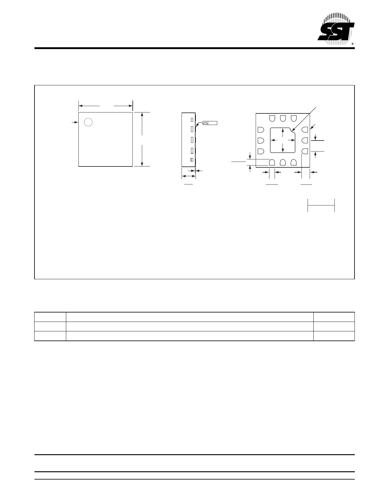
PACKAGING DIAGRAMS
Data Sheet
Pin 1
(Laser
Engraved)
TOP VIEW
2.00
0.05
2.00
0.05
SIDE VIEW
0.075
0.05 Max
0.265
0.165
0.60
0.50
BOTTOM VIEW
See notes
2 and 3
Pin 1
0.92
0.4 BSC
0.25 0.34
0.15 0.24
1mm
12-uqfn-2x2-QUB-1.0
Note 1. Similar to JEDEC JEP95 UQFN/USON variants, though number of contacts and some dimensions are different.
2. From the bottom view, the pin 1 in dicator may be either a curved indent or a 45-degree chamfer.
3. The external paddle is electrically connected to the die back-side and to VSS.
This paddle must be soldered to the PC board; it is required to connect this paddle to the VSS of the unit.
Connection of this paddle to any other voltage potential will result in shorts and electrical malfunction of
the device.
4. Untoleranced dimensions are nominal target dimensions.
5. All linear dimensions are in millimeters (max/min).
FIGURE 11: 12-contact Ultra-thin Quad Flat No-lead (UQFN)
SST Package Code: QUB
TABLE 4: Revision History
Revision
00
01
•
•
Description
Initial Release of Data Sheet
Updated Features on page 1; Table 2 on page 4; and Figures 3-5, 7,8, and 10.
Date
Jul 2010
Jan 2011
©2011 Silicon Storage Technology, Inc.
Silicon Storage Technology, Inc.
www.SuperFlash.com or www.sst.com
11
S71428-01-000
01/11
11 Page | ||
| Páginas | Total 11 Páginas | |
| PDF Descargar | [ Datasheet SST11CP15.PDF ] | |
Hoja de datos destacado
| Número de pieza | Descripción | Fabricantes |
| SST11CP15 | 4.9-5.8 GHz High-Linearity Power Amplifier | Silicon Storage Technology |
| SST11CP15E | 4.9-5.9 GHz High-Linearity Power Amplifier | Microchip |
| SST11CP16 | 5.1-5.9 GHz High-Linearity Power Amplifier | Microchip |
| Número de pieza | Descripción | Fabricantes |
| SLA6805M | High Voltage 3 phase Motor Driver IC. |
Sanken |
| SDC1742 | 12- and 14-Bit Hybrid Synchro / Resolver-to-Digital Converters. |
Analog Devices |
|
DataSheet.es es una pagina web que funciona como un repositorio de manuales o hoja de datos de muchos de los productos más populares, |
| DataSheet.es | 2020 | Privacy Policy | Contacto | Buscar |
