|
|
|
PDF 34905 Data sheet ( Hoja de datos )
| Número de pieza | 34905 | |
| Descripción | System Basis Chip | |
| Fabricantes | Freescale Semiconductor | |
| Logotipo | ||
Hay una vista previa y un enlace de descarga de 34905 (archivo pdf) en la parte inferior de esta página. Total 30 Páginas | ||
|
No Preview Available !
Freescale Semiconductor
Technical Data
Document Number: MC34903_4_5
Rev. 4.0, 10/2013
System Basis Chip with CAN
High Speed and LIN Interface
I3n34d49u90s03t3/r4/i/a5l
The 34903/4/5 is the second generation family of the System Basis
Chip (SBC). It combines several features and enhances present
module designs. The device works as an advanced power
management unit for the MCU with additional integrated circuits such
as sensors and CAN transceivers. It has a built-in enhanced high-speed
CAN interface (ISO11898-2 and -5) with local and bus failure
diagnostics, protection, and fail-safe operation modes. The SBC may
include zero or one LIN 2.1 interface with LIN output pin switches. It
includes up to four wake-up input pins that can also be configured as
output drivers for flexibility. This device is powered by SMARTMOS
technology.
SYSTEM BASIS CHIP
This device implements multiple Low-power (LP) modes, with very
low-current consumption. In addition, the device is part of a family
concept where pin compatibility adds versatility to module design.
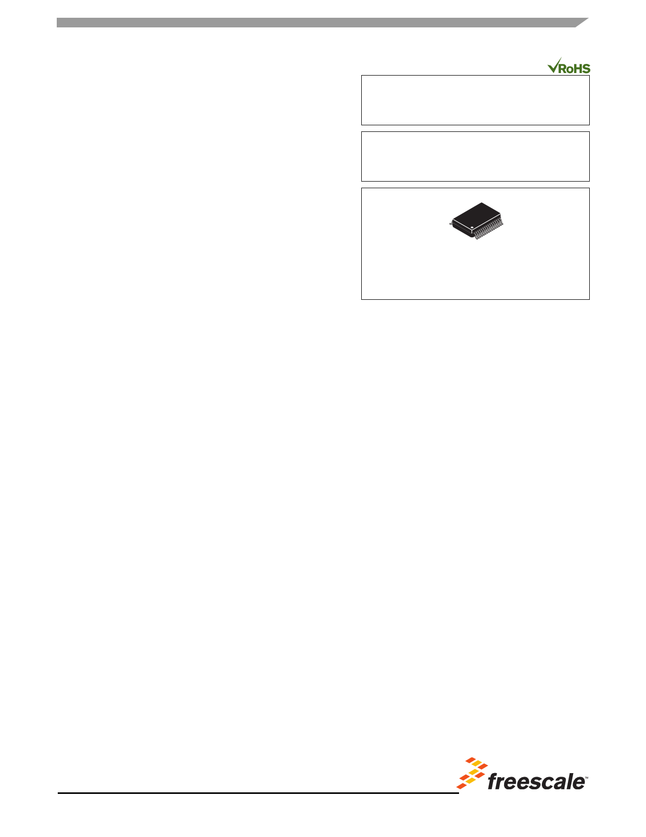
EK Suffix (Pb-free)
98ASA10556D
32-PIN SOIC
The 34903/4/5 also implements an innovative and advanced fail-safe
state machine and concept solution.
Applications
Features
• Industrial process control
• Voltage regulator for MCU, 5.0 or 3.3 V, part number selectable, with
possibility of usage external PNP to extend current capability and
share power dissipation
• Voltage, current, and temperature protection
• Automation
• Motor control
• Robotics
• Extremely low quiescent current in LP modes
• Fully-protected embedded 5.0 V regulator for the CAN driver
• Multiple undervoltage detections to address various MCU
specifications and system operation modes (i.e. cranking)
• Auxiliary 5.0 or 3.3 V SPI configurable regulator, for additional ICs,
with overcurrent detection and undervoltage protection
• MUX output pin for device internal analog signal monitoring and
power supply monitoring
• Advanced SPI, MCU, ECU power supply, and critical pins
diagnostics and monitoring.
• Multiple wake-up sources in LP modes: CAN or LIN bus,
I/O transition, automatic timer, SPI message, and VDD overcurrent
detection.
• ISO11898-5 high-speed CAN interface compatibility for baud rates of
40 kb/s to 1.0 Mb/s
• Scalable product family of devices ranging from 0 to 1 LIN,
compatible to J2602-2 and LIN 2.1
Freescale Semiconductor, Inc. reserves the right to change the detail specifications,
as may be required, to permit improvements in the design of its products.
© Freescale Semiconductor, Inc., 2013. All rights reserved.
1 page 
DEVICE VARIATIONS
DEVICE VARIATIONS
Table 1. MC34905 Device Variations - (All devices rated at TA = -40 TO 125 °C)
Freescale Part Number
MC34905S (Single LIN)
Version
VDD Output
Voltage
LIN Wake-up Input / LIN Master
Interface(s)
Termination
MC34905CS3EK/R2
MC34905CS5EK/R2
C 3.3 V
C 5.0 V
3 Wake-up + 1 LIN terms
1 or
4 Wake-up + no LIN terms
Package
SOIC 32 pin
exposed pad
VAUX VSENSE MUX
Yes Yes Yes
Table 2. MC34904 Device Variations - (All devices rated at TA = -40 TO 125 °C)
Freescale Part Number
Version
VDD Output
Voltage
LIN Wake-up Input / LIN Master
Interface(s)
Termination
MC34904
MC34904C3EK/R2
MC34904C5EK/R2
C 3.3 V
C 5.0 V
0
4 Wake-up
Package
SOIC 32 pin
exposed pad
VAUX VSENSE MUX
Yes Yes Yes
Table 3. MC34903 Device Variations - (All devices rated at TA = -40 TO 125 °C)
Freescale Part Number
Version
VDD Output
Voltage
LIN Wake-up Input / LIN Master
Interface(s)
Termination
MC34903S (Single LIN)
MC34903CS3EK/R2
MC34903CS5EK/R2
C 3.3 V
C 5.0 V
2 Wake-up + 1 LIN terms
1 or
3 Wake-up + no LIN terms
MC34903P
MC34903CP5EK/R2
MC34903CP3EK/R2
5.0 V
C
3.3 V
0
3 Wake-up
Package
SOIC 32 pin
exposed pad
SOIC 32 pin
exposed pad
VAUX VSENSE MUX
No Yes Yes
No Yes Yes
Analog Integrated Circuit Device Data
Freescale Semiconductor
34903/4/5
5
5 Page 
PIN DEFINITIONS
Table 4. 34903/4/5 Pin Definitions (continued)
32 Pin
34905S
32 Pin
34904
32 Pin 32 Pin
34903S 34903P
Pin Name
Pin
Function
Formal
Name
Definition
32 32
1
1
EX PAD EX PAD EX PAD EX PAD
VB
GND
Output Voltage Base Base output pin for connection to the external PNP pass transistor
Ground
Ground Ground
Analog Integrated Circuit Device Data
Freescale Semiconductor
34903/4/5
11
11 Page | ||
| Páginas | Total 30 Páginas | |
| PDF Descargar | [ Datasheet 34905.PDF ] | |
Hoja de datos destacado
| Número de pieza | Descripción | Fabricantes |
| 34903 | System Basis Chip | Freescale Semiconductor |
| 34904 | System Basis Chip | Freescale Semiconductor |
| 34905 | System Basis Chip | Freescale Semiconductor |
| Número de pieza | Descripción | Fabricantes |
| SLA6805M | High Voltage 3 phase Motor Driver IC. |
Sanken |
| SDC1742 | 12- and 14-Bit Hybrid Synchro / Resolver-to-Digital Converters. |
Analog Devices |
|
DataSheet.es es una pagina web que funciona como un repositorio de manuales o hoja de datos de muchos de los productos más populares, |
| DataSheet.es | 2020 | Privacy Policy | Contacto | Buscar |