|
|
|
PDF HMC5883 Data sheet ( Hoja de datos )
| Número de pieza | HMC5883 | |
| Descripción | 3-Axis Digital Compass IC | |
| Fabricantes | Honeywell | |
| Logotipo | ||
Hay una vista previa y un enlace de descarga de HMC5883 (archivo pdf) en la parte inferior de esta página. Total 19 Páginas | ||
|
No Preview Available !
3-Axis Digital Compass IC
HMC5883
Advanced Information
The Honeywell HMC5883 is a surface mount multi-chip module designed for low
field magnetic sensing with a digital interface for applications such as low cost
compassing and magnetometry. The HMC5883 includes our state of the art,
high-resolution HMC118X series magneto-resistive sensors plus Honeywell
developed ASIC containing amplification, automatic degaussing strap drivers,
offset cancellation, 12-bit ADC that enables 1° to 2° compass heading accuracy.
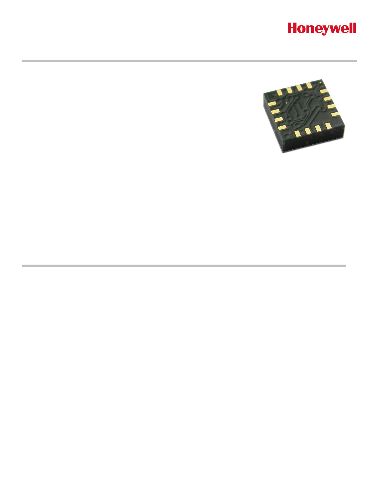
The I2C serial bus allows for easy interface. The HMC5883 is a 3.0x3.0x0.9mm
surface mount 16-pin leadless chip carrier (LCC). Applications for the HMC5883
include Mobile Phones, Netbooks, Consumer Electronics, Auto Navigation
Systems, and Personal Navigation Devices.
The HMC5883 utilizes Honeywell’s Anisotropic Magnetoresistive (AMR) technology that provides advantages over other
magnetic sensor technologies. These anisotropic, directional sensors feature precision in-axis sensitivity and linearity,
solid-state construction with very low cross-axis sensitivity designed to measure both direction and magnitude of Earth’s
magnetic fields, from milli-gauss to 8 gauss. Honeywell’s Magnetic Sensors are among the most sensitive and reliable
low-field sensors in the industry.
FEATURES
3-Axis Magnetoresistive Sensors and
ASIC in a 3.0x3.0x0.9mm LCC Surface
Mount Package
12-Bit ADC Coupled with Low Noise
AMR Sensors Achieves 5 milli-Gauss
Resolution in ±8 Gauss Fields
Built-In Self Test
Low Voltage Operations (1.6 to 3.3V)
Built-In Strap Drive Circuits
I2C Digital Interface
Lead Free Package Construction
Wide Magnetic Field Range (+/-8 Oe)
Software and Algorithm Support
Available
Fast 116 Hz Maximum Output Rate
BENEFITS
Small Size for Highly Integrated Products. Just Add a Micro-
Controller Interface, Plus Two External SMT Capacitors
Designed for High Volume, Cost Sensitive OEM Designs
Easy to Assemble & Compatible with High Speed SMT Assembly
Enables 1° to 2° Degree Compass Heading Accuracy
Enables Low-Cost Functionality Test after Assembly in Production
Compatible for Battery Powered Applications
Set/Reset and Offset Strap Drivers for Degaussing, Self Test, and
Offset Compensation
Popular Two-Wire Serial Data Interface for Consumer Electronics
RoHS Compliance
Sensors Can Be Used in Strong Magnetic Field Environments with a
1° to 2° Degree Compass Heading Accuracy
Compassing Heading, Hard Iron, Soft Iron, and Auto Calibration
Libraries Available
Enables Pedestrian Navigation and LBS Applications
Free Datasheet http://www.Datasheet4U.com
1 page 
HMC5883
MOUNTING CONSIDERATIONS
The following is the recommend printed circuit board (PCB) footprint for the HMC5883.
PCB Pad Definition and Traces
The HMC5883 is a fine pitch LCC package with a 0.50mm pin pitch (spacing), with the pin pads defined as 0.325mm by
0.25mm in size. PCB pads are recommended to be oversized by 0.025mm from each pad for a short dimension oversize
of 0.05mm. The interior PCB pad is recommended to be 0.05mm oversized per pin with an exterior oversize of 0.20mm
for proper package centering and to permit test probing. Size the traces between the HMC5883 and the external
capacitors (C1 and C2) to handle the 1 ampere peak current pulses with low voltage drop on the traces.
Stencil Design and Solder Paste
A 4 mil stencil and 100% paste coverage is recommended for the electrical contact pads.
Pick and Place
Placement is machine dependant and no restrictions are recommended, and have been tested with mechanical centering.
Placement force should be equivalent 1206 SMT resistors and enough force should be used to squeeze the paste out
from the package/contact pad overlap and to keep the package pin contacts vertical.
Reflow Assembly
This device is classified as MSL 3 with 260 C peak reflow temperature. A baking process (125 C, 24 hrs) is required if
device is not kept continuously in a dry (< 10% RH) environment before assembly. No special reflow profile is required for
the HMC5883 which is compatible with lead eutectic and lead-free solder paste reflow profiles. Honeywell recommends
the adherence to solder paste manufacturer’s guidelines.
INTERNAL SCHEMATIC DIAGRAM
HMC5883
www.honeywell.com
5
Free Datasheet http://www.Datasheet4U.com
5 Page 
HMC5883
REGISTERS
This device is controlled and configured via a number of on-chip registers, which are described in this section. In the
following descriptions, set implies a logic 1, and reset or clear implies a logic 0, unless stated otherwise.
Register List
The table below lists the registers and their access. All address locations are 8 bits.
Address Location
00
01
02
03
04
05
06
07
08
09
10
11
12
Name
Configuration Register A
Configuration Register B
Mode Register
Data Output X MSB Register
Data Output X LSB Register
Data Output Z MSB Register
Data Output Z LSB Register
Data Output Y MSB Register
Data Output Y LSB Register
Status Register
Identification Register A
Identification Register B
Identification Register C
Access
Read/Write
Read/Write
Read/Write
Read
Read
Read
Read
Read
Read
Read
Read
Read
Read
Table 5: Register List
Register Access
This section describes the process of reading from and writing to this device. The devices uses an address pointer to
indicate which register location is to be read from or written to. These pointer locations are sent from the master to this
slave device and succeed the 7-bit address plus 1 bit read/write identifier.
To minimize the communication between the master and this device, the address pointer updated automatically without
master intervention. This automatic address pointer update has two additional features. First when address 12 or higher
is accessed the pointer updates to address 00 and secondly when address 09 is reached, the pointer rolls back to
address 03. Logically, the address pointer operation functions as shown below.
If (address pointer = 09) then address pointer = 03
Else if (address pointer >= 12) then address pointer = 0
Else (address pointer) = (address pointer) + 1
The address pointer value itself cannot be read via the I2C bus.
Any attempt to read an invalid address location returns 0’s, and any write to an invalid address location or an undefined bit
within a valid address location is ignored by this device.
To move the address pointer to a random register location, first issue a “write” to that register location with no data byte
following the commend. For example, to move the address pointer to register 10, send 0x3C 0x0A.
www.honeywell.com
11
Free Datasheet http://www.Datasheet4U.com
11 Page | ||
| Páginas | Total 19 Páginas | |
| PDF Descargar | [ Datasheet HMC5883.PDF ] | |
Hoja de datos destacado
| Número de pieza | Descripción | Fabricantes |
| HMC5883 | 3-Axis Digital Compass IC | Honeywell |
| HMC5883L | 3-Axis Digital Compass IC | Honeywell |
| HMC588LC4B | WIDEBAND MMIC VCO w/ BUFFER AMPLIFIER | Hittite Microwave |
| Número de pieza | Descripción | Fabricantes |
| SLA6805M | High Voltage 3 phase Motor Driver IC. |
Sanken |
| SDC1742 | 12- and 14-Bit Hybrid Synchro / Resolver-to-Digital Converters. |
Analog Devices |
|
DataSheet.es es una pagina web que funciona como un repositorio de manuales o hoja de datos de muchos de los productos más populares, |
| DataSheet.es | 2020 | Privacy Policy | Contacto | Buscar |