|
|
|
PDF IRS20965 Data sheet ( Hoja de datos )
| Número de pieza | IRS20965 | |
| Descripción | CLASS D AUDIO DRIVER | |
| Fabricantes | International Rectifier | |
| Logotipo | ||
Hay una vista previa y un enlace de descarga de IRS20965 (archivo pdf) en la parte inferior de esta página. Total 16 Páginas | ||
|
No Preview Available !
IRS20965
Features
Hi-side and Lo-side independent floating PWM
input
Programmable bidirectional over-current
detection with self-reset function
Over current sensing output
Shoot-through prevention logic
High noise immunity
±100 V ratings deliver up to 500 W in output
power
3.3 V / 5 V logic compatible input
Operates up to 800 kHz
CLASS D AUDIO DRIVER
Product Summary
VOFFSET (max)
Gate driver
Io+
Io-
Propagation delay
OC protection delay (max)
Shutdown delay (max)
100 V
2.0 A
2.0 A
120 ns
500 ns
250 ns
Typical Applications
Class D audio amplifier
Half bridge converter with digital controller
Package Options
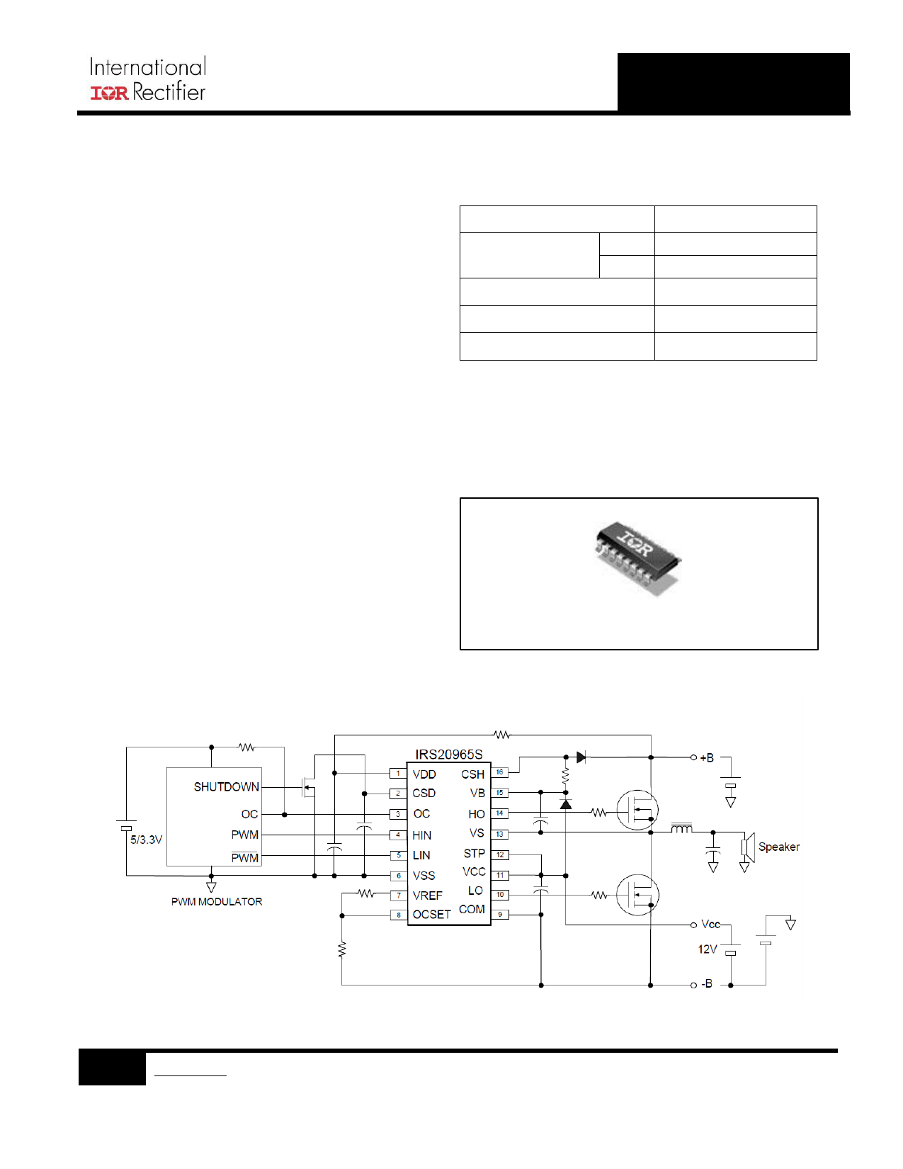
Typical Connection Diagram
16-Lead SOIC
(Please refer to Lead Assignments for correct pin configuration. This diagram shows electrical connections only.)
1 www.irf.com © 2014 International Rectifier
February 21, 2014
http://www.Datasheet4U.com
1 page 
IRS20965
Absolute Maximum Ratings
Absolute Maximum Ratings indicate sustained limits beyond which damage to the device may occur. All voltage
parameters are absolute voltages referenced to VSS; all currents are defined positive into any lead. The Thermal
Resistance and Power Dissipation ratings are measured under board mounted and still air conditions.
Symbol
VB
VS
VHO
VCSH
VCC
VLO
VDD
VSS
VHIN
VLIN
VCSD
VOC
VOCSET
VREF
IDDZ
ICCZ
IBSZ
IOREF
dVs/dt
dVss/dt
dVss/dt
Pd
RthJA
TJ
TS
TL
Definition
High side floating supply voltage
High side floating supply voltage †
High side floating output voltage
CSH pin input voltage
Low side fixed supply voltage †
Low side output voltage
Floating input supply voltage
Floating input supply voltage †
PWM input voltage
PWM input voltage
CSD pin input voltage
OC pin input voltage
OCSET pin input voltage
VREF pin voltage
Floating input supply zener clamp current †
Low side supply zener clamp current †
Floating supply zener clamp current †
Reference output current
Allowable Vs voltage slew rate
Allowable Vss voltage slew rate ††
Allowable Vss voltage slew rate upon power-up †††
Maximum power dissipation
Thermal resistance, Junction to ambient
Junction Temperature
Storage Temperature
Lead temperature (Soldering, 10 seconds)
Min.
-0.3
VB-20
Vs-0.3
Vs-0.3
-0.3
-0.3
-0.3
(See IDDZ)
VSS -0.3
VSS -0.3
VSS -0.3
VSS -0.3
-0.3
-0.3
-
-
-
-
-
-
-
-
-
-
-55
-
Max.
215
VB+0.3
VB+0.3
VB+0.3
20
VCC +0.3
210
VDD+0.3
VDD+0.3
VDD+0.3
VDD+0.3
VDD+0.3
VCC +0.3
VCC +0.3
10
10
10
5
50
50
50
1.0
115
150
150
300
Units
V
mA
V/ns
V/ms
W
˚C/W
˚C
† VDD - VSS, VCC - COM, and VB - VS contain internal shunt zener diodes. Please note that the voltage
ratings of these can be limited by the clamping current.
†† For the rising and falling edges of step signal of 10V. VSS = 15V to 200V.
††† VSS ramps up from 0V to 200V.
5 www.irf.com © 2014 International Rectifier
February 21, 2014
http://www.Datasheet4U.com
5 Page 
Functional Block Diagram
IRS20965
11 www.irf.com © 2014 International Rectifier
February 21, 2014
http://www.Datasheet4U.com
11 Page | ||
| Páginas | Total 16 Páginas | |
| PDF Descargar | [ Datasheet IRS20965.PDF ] | |
Hoja de datos destacado
| Número de pieza | Descripción | Fabricantes |
| IRS20965 | CLASS D AUDIO DRIVER | International Rectifier |
| Número de pieza | Descripción | Fabricantes |
| SLA6805M | High Voltage 3 phase Motor Driver IC. |
Sanken |
| SDC1742 | 12- and 14-Bit Hybrid Synchro / Resolver-to-Digital Converters. |
Analog Devices |
|
DataSheet.es es una pagina web que funciona como un repositorio de manuales o hoja de datos de muchos de los productos más populares, |
| DataSheet.es | 2020 | Privacy Policy | Contacto | Buscar |