|
|
|
PDF MRF8S26120HR3 Data sheet ( Hoja de datos )
| Número de pieza | MRF8S26120HR3 | |
| Descripción | RF Power Field Effect Transistor | |
| Fabricantes | Motorola Semiconductors | |
| Logotipo | ||
Hay una vista previa y un enlace de descarga de MRF8S26120HR3 (archivo pdf) en la parte inferior de esta página. Total 15 Páginas | ||
|
No Preview Available !
Freescale Semiconductor
Technical Data
Document Number: MRF8S26120H
www.DRaetavS.he0e,t46U/.2co0m10
RF Power Field Effect Transistors
N--Channel Enhancement--Mode Lateral MOSFETs
Designed for W--CDMA and LTE base station applications with frequencies
from 2620 to 2690 MHz. Can be used in Class AB and Class C for all typical
cellular base station modulation formats.
• Typical Single--Carrier W--CDMA Performance: VDD = 28 Volts,
IBDaQn=dw9i0d0thm=A3,.P84ouMt =H2z,8InWpautttsSAigvnga.l,
IQ Magnitude
PAR = 7.5 dB
Clipping,
@ 0.01%
Channel
Probability
on CCDF.
Frequency
Gps
(dB)
ηD Output PAR ACPR
(%)
(dB)
(dBc)
2620 MHz
2655 MHz
2690 MHz
15.5
15.5
15.6
31.5
31.1
31.1
6.3 --38.0
6.3 --37.3
6.2 --36.7
MRF8S26120HR3
MRF8S26120HSR3
2620--2690 MHz, 28 W AVG., 28 V
W--CDMA, LTE
LATERAL N--CHANNEL
RF POWER MOSFETs
• Capable of Handling 10:1 VSWR, @ 32 Vdc, 2655 MHz, 135 Watts CW
Output Power (3 dB Input Overdrive from Rated Pout)
• Typical Pout @ 1 dB Compression Point ≃ 110 Watts CW
Features
• 100% PAR Tested for Guaranteed Output Power Capability
• Characterized with Series Equivalent Large--Signal Impedance Parameters
and Common Source S--Parameters
• Internally Matched for Ease of Use
• Integrated ESD Protection
• Greater Negative Gate--Source Voltage Range for Improved Class C
Operation
• Designed for Digital Predistortion Error Correction Systems
• Optimized for Doherty Applications
• RoHS Compliant
• In Tape and Reel. R3 Suffix = 250 Units per 56 mm, 13 inch Reel.
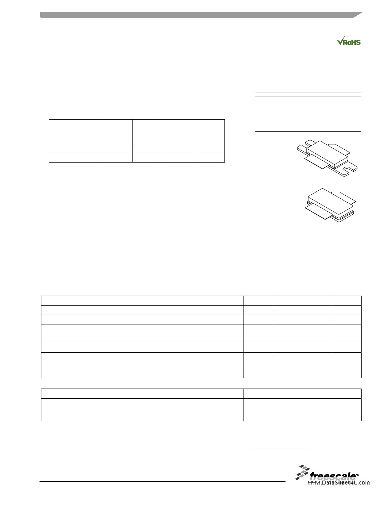
CASE 465--06, STYLE 1
NI--780
MRF8S26120HR3
CASE 465A--06, STYLE 1
NI--780S
MRF8S26120HSR3
Table 1. Maximum Ratings
Rating
Symbol
Value
Unit
Drain--Source Voltage
Gate--Source Voltage
Operating Voltage
Storage Temperature Range
Case Operating Temperature
Operating Junction Temperature (1,2)
CW Operation @ TC = 25°C
Derate above 25°C
VDSS
VGS
VDD
Tstg
TC
TJ
CW
--0.5, +65
--6.0, +10
32, +0
--65 to +150
150
225
141
0.78
Vdc
Vdc
Vdc
°C
°C
°C
W
W/°C
Table 2. Thermal Characteristics
Characteristic
Symbol
Value (2,3)
Unit
Thermal Resistance, Junction to Case
Case Temperature 72°C, 28 W CW, 28 Vdc, IDQ = 900 mA, 2690 MHz
Case Temperature 85°C, 110 W CW(4), 28 Vdc, IDQ = 900 mA, 2690 MHz
RθJC
0.53
0.47
°C/W
1. Continuous use at maximum temperature will affect MTTF.
2. MTTF calculator available at http://www.freescale.com/rf. Select Software & Tools/Development Tools/Calculators to access MTTF
calculators by product.
3. Refer to AN1955, Thermal Measurement Methodology of RF Power Amplifiers. Go to http://www.freescale.com/rf.
Select Documentation/Application Notes -- AN1955.
4. Exceeds recommended operating conditions. See CW operation data in Maximum Ratings table.
© Freescale Semiconductor, Inc., 2010. All rights reserved.
RF Device Data
Freescale Semiconductor
MRF8S26120HR3 MRF8S26120HSR3
1
1 page 
TYPICAL CHARACTERISTICS
16 32
15.9
VDD = 28 Vdc, Pout = 28 W (Avg.), IDQ = 900 mA
Single--Carrier W--CDMA, 3.84 MHz Channel Bandwidth
31.8
15.8 Input Signal PAR = 7.5 dB @ 0.01% Probability on CCDF 31.6
15.7
15.6 ηD
15.5 Gps
15.4
31.4
31.2
IRL --35
--36
15.3 --37
15.2
ACPR
15.1
PARC
--38
--39
15 --40
2570 2590 2610 2630 2650 2670 2690 2710 2730
f, FREQUENCY (MHz)
Figure 2. Output Peak--to--Average Ratio Compression (PARC)
Broadband Performance @ Pout = 28 Watts Avg.
www.DataSheet4U.com
--13 --1
--14 --1.1
--15 --1.2
--16 --1.3
--17 --1.4
--18 --1.5
--10
VDD = 28 Vdc, Pout = 80 W (PEP), IDQ = 900 mA
Two--Tone Measurements
--20 (f1 + f2)/2 = Center Frequency of 2655 MHz
IM3--U
--30
IM3--L
--40 IM5--L
--50
IM7--L
IM5--U
IM7--U
--60
1
10 100
TWO--TONE SPACING (MHz)
Figure 3. Intermodulation Distortion Products
versus Two--Tone Spacing
16.5 1
16 0
15.5 --1
ACPR
ηD
60
50
40
--25
--30
--35
15 --2 --1 dB = 25 W
14.5 --3
--2 dB = 35 W
--3 dB = 45 W
Gps
PARC
30
20
--40
--45
14 --4 VDD = 28 Vdc, IDQ = 900 mA, f = 2655 MHz
10 --50
Single--Carrier W--CDMA, 3.84 MHz Channel Bandwidth
13.5
--5 Input Signal PAR = 7.5 dB @ 0.01% Probability on CCDF
0
--55
10 20 30 40
50 60
Pout, OUTPUT POWER (WATTS)
Figure 4. Output Peak--to--Average Ratio
Compression (PARC) versus Output Power
RF Device Data
Freescale Semiconductor
MRF8S26120HR3 MRF8S26120HSR3
5
5 Page 
www.DataSheet4U.com
RF Device Data
Freescale Semiconductor
MRF8S26120HR3 MRF8S26120HSR3
11
11 Page | ||
| Páginas | Total 15 Páginas | |
| PDF Descargar | [ Datasheet MRF8S26120HR3.PDF ] | |
Hoja de datos destacado
| Número de pieza | Descripción | Fabricantes |
| MRF8S26120HR3 | RF Power Field Effect Transistor | Motorola Semiconductors |
| MRF8S26120HR3 | RF Power Field Effect Transistor | Motorola Semiconductors |
| Número de pieza | Descripción | Fabricantes |
| SLA6805M | High Voltage 3 phase Motor Driver IC. |
Sanken |
| SDC1742 | 12- and 14-Bit Hybrid Synchro / Resolver-to-Digital Converters. |
Analog Devices |
|
DataSheet.es es una pagina web que funciona como un repositorio de manuales o hoja de datos de muchos de los productos más populares, |
| DataSheet.es | 2020 | Privacy Policy | Contacto | Buscar |