|
|
PDF LTC4280 Data sheet ( Hoja de datos )
| Número de pieza | LTC4280 | |
| Descripción | Hot Swap Controller | |
| Fabricantes | Linear Technology | |
| Logotipo |  |
|
Hay una vista previa y un enlace de descarga de LTC4280 (archivo pdf) en la parte inferior de esta página. Total 28 Páginas | ||
|
No Preview Available !
www.DataSheet4U.com
LTC4280
Hot Swap Controller with
I2C Compatible Monitoring
FEATURES
n Allows Safe Insertion into Live Backplane
n 8-Bit ADC Monitors Current and Voltage
n I2C/SMBus Interface
n Wide Operating Voltage Range: 2.9V to 15V
n Adjustable Overcurrent Filter Time
n High Side Drive for External N-Channel MOSFET
n No External Gate Capacitor Required
n Input Overvoltage/Undervoltage Protection
n Optional Latchoff or Auto-Retry After Faults
n Alerts Host After Faults
n Inrush Current Limit with Foldback
n Available in 24-Pin 4mm × 5mm QFN Package
APPLICATIONS
n Live Board Insertion
n Electronic Circuit Breakers
n Computers, Servers
n Platform Management
L, LT, LTC, LTM, Linear Technology, the Linear logo and Hot Swap are registered trademarks of
Linear Technology Corporation. All other trademarks are the property of their respective owners.
DESCRIPTION
The LTC®4280 Hot Swap™ controller allows a board to be
safely inserted and removed from a live backplane. Using
an external N-channel pass transistor, board supply voltage
and inrush current are ramped up at an adjustable rate.
An I2C interface and onboard ADC allow for monitoring
of load current, voltage and fault status.
The device features adjustable analog foldback current
limit and a FILTER pin which configures the time spent in
overcurrent before declaring a fault. An I2C interface may
configure the part to latch off or automatically restart after
the LTC4280 detects a current limit fault.
The controller has additional features to interrupt the host
when a fault has occurred, notify when output power is
good, detect insertion of a load card, and power-up either
automatically upon insertion or wait for an I2C command
to turn on.
TYPICAL APPLICATION
12V Application with 5A Circuit Breaker
12V
SDA
SCL
ALERT
GND
BACKPLANE PLUG-IN
CARD
34.8k
0.1μF
0.005Ω
FDC653N
+
VOUT
12V
CL 30.1k
10Ω
1.18k
P6KE16A
3.4k
INTVCC
UV VDD SENSE+ SENSE– GATE SOURCE
OV FB
SDAO
SDAI
SCL
ALERT
LTC4280
EN
ADIN
GPIO
INTVCC ON TIMER FILTER GND
0.1μF
47nF
3.57k
INTVCC
24k
4280 TA01
Start-Up Waveform
VDD
10V/DIV
INRUSH
CURRENT
2.5A/DIV
VOUT
10V/DIV
VGPIO
(POWERGOOD)
10V/DIV
CONTACT
BOUNCE
CL = 12000μF
50ms/DIV
4280 TA02
4280f
1
1 page 
www.DataSheet4U.com
LTC4280
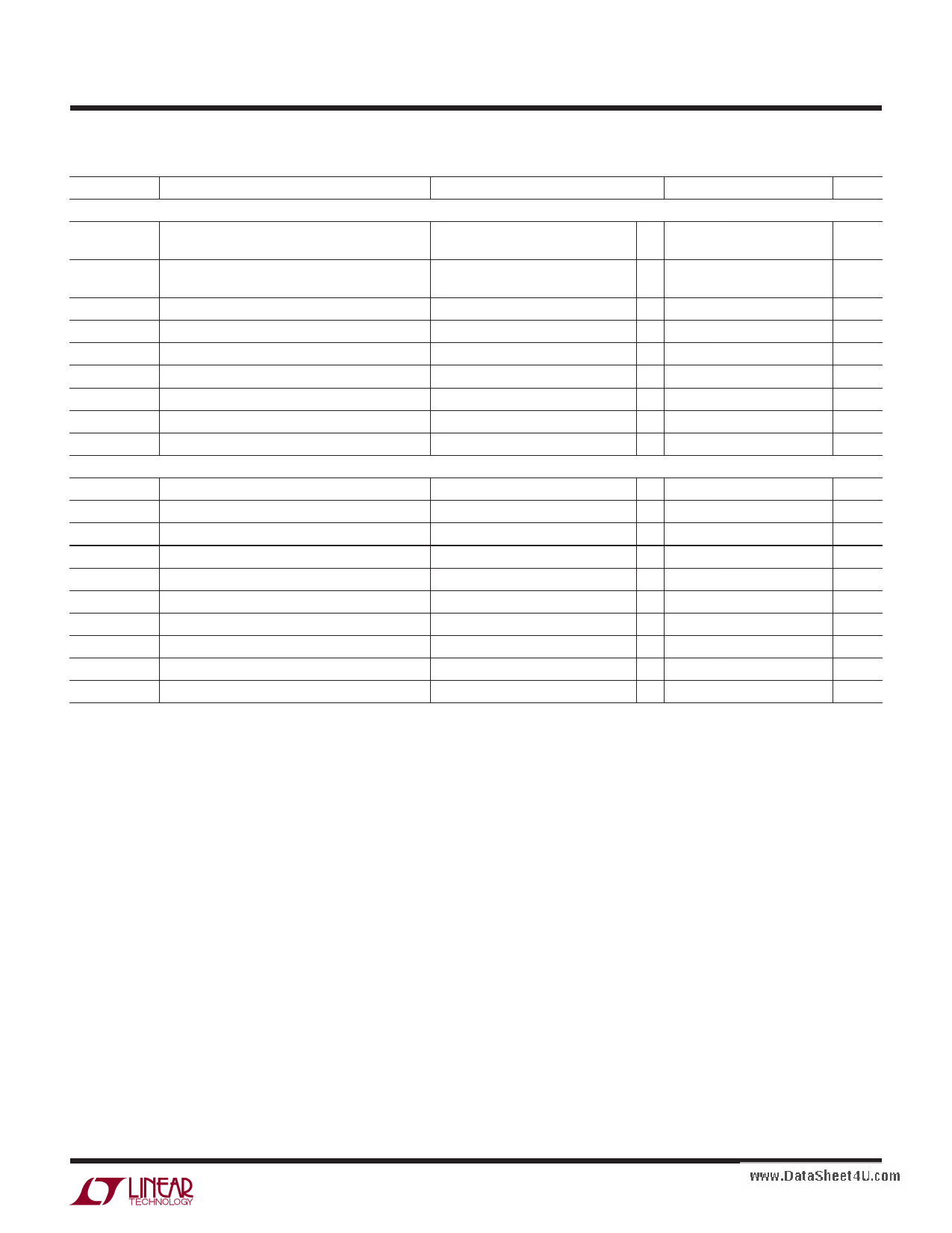
ELECTRICAL CHARACTERISTICS The l denotes the specifications which apply over the full operating
temperature range, otherwise specifications are at TA = 25°C. VDD = 12V unless otherwise noted.
SYMBOL
PARAMETER
CONDITIONS
MIN TYP MAX UNITS
I2C Interface
VADR(H)
ADR0, ADR1, ADR2 Input High Voltage
l INTVCC INTVCC INTVCC
–0.8 –0.4 –0.2
V
IADR(IN,Z)
ADR0, ADR1, ADR2 Hi-Z Input Current
ADR0, ADR1, ADR2 = 0.8V
l
ADR0, ADR1, ADR2 = INTVCC – 0.8V l
3
–3 μA
μA
VADR(L)
ADR0, ADR1, ADR2 Input Low Voltage
l 0.2 0.4 0.8
V
IADR(IN)
IALERT
VALERT(OL)
ADR0, ADR1, ADR2 Input Current
ALERT Input Current
ALERT Output Low Voltage
ADR0, ADR1, ADR2 = 0V, INTVCC
ALERT = 6.5V
l –80
l
80
±1
IALERT = 3mA
l 0.2 0.4
μA
μA
V
VSDA,SCL(TH) SDA, SCL Input Threshold
l 1.3 1.7 1.9
V
ISDA,SCL(OH)
SDA, SCL Input Current
SCL, SDA = 6.5V
l
±1 μA
VSDA(OL)
SDA Output Low Voltage
I2C Interface Timing
ISDA = 3mA
l
0.2 0.4
V
fSCL(MAX)
SCL Clock Frequency
Operates with fSCL ≤ fSCL(MAX)
l 400 1000
kHz
tBUF(MIN)
Bus Free Time Between Stop/Start Condition
l
0.12 1.3
μs
tHD,STA(MIN)
Hold Time After (Repeated) Start Condition
l
30 600
ns
tSU,STA(MIN)
Repeated Start Condition Set-Up Time
l
30 600
ns
tSU,STO(MIN)
Stop Condition Set-Up Time
l
140 600
ns
tHD,DAT(MIN)
Data Hold Time (Input)
l
30 100
ns
tHD,DATO
Data Hold Time (Output)
l 300 500 900
ns
tSU,DAT(MIN)
Data Set-Up Time
l
30 600
ns
tSP Suppressed Spike Pulse Width
l 50
110 250
ns
CX SCL, SDA Input Capacitance
SDAI Tied to SDAO (Note 6)
l
10 pF
Note 1: Stresses beyond those listed under Absolute Maximum Ratings
may cause permanent damage to the device. Exposure to any Absolute
Maximum Rating condition for extended periods may affect device
reliability and lifetime.
Note 2: All currents into pins are positive; all voltages are referenced to
GND unless otherwise specified.
Note 4: Offset error is the offset voltage measured from 1LSB when the
output code flickers between 0000 0000 and 0000 0001.
Note 5: Integral nonlinearity is defined as the deviation of a code from a
precise analog input voltage. Maximum specifications are limited by the
LSB step size and the single shot measurement. Typical specifications are
measured from the 1/4, 1/2 and 3/4 areas of the quantization band.
Note 3: An internal clamp limits the GATE pin to a minimum of 5V above
SOURCE. Driving this pin to voltages beyond the clamp may damage the device.
Note 6: Guaranteed by design and not subject to test.
4280f
5
5 Page 
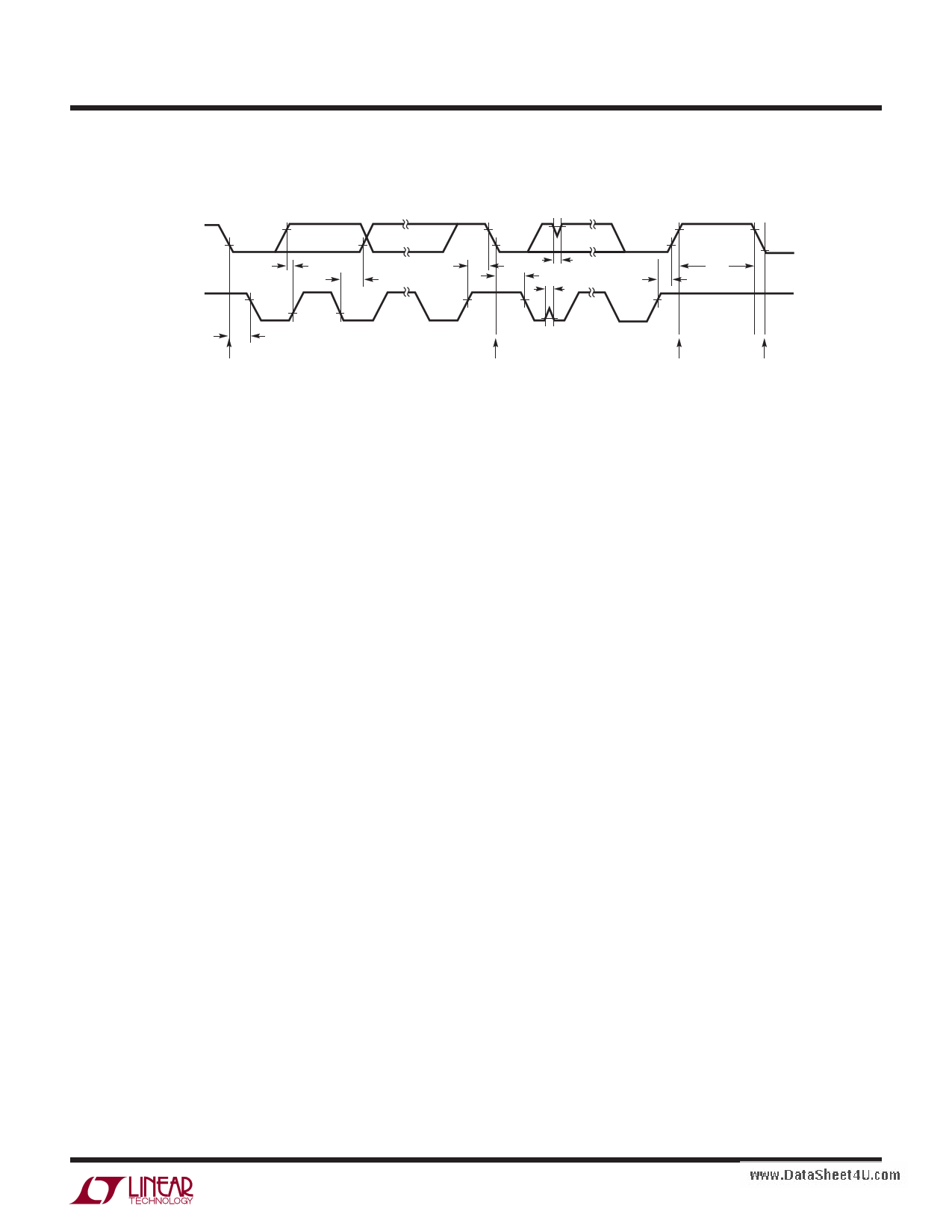
TIMING DIAGRAM
www.DataSheet4U.com
LTC4280
SDAI/SDAO
SCL
tHD, STA
START
CONDITION
tSU, DAT
tHD, DATO,
tHD, DATI
tSU, STA
tSP
tHD, STA
tSP
tSU, STO
tBUF
4280 TD01
REPEATED START
CONDITION
STOP
CONDITION
START
CONDITION
4280f
11
11 Page | ||
| Páginas | Total 28 Páginas | |
| PDF Descargar | [ Datasheet LTC4280.PDF ] | |
Hoja de datos destacado
| Número de pieza | Descripción | Fabricantes |
| LTC4280 | Hot Swap Controller | Linear Technology |
| LTC4282 | High Current Hot Swap Controller | Linear Technology |
| Número de pieza | Descripción | Fabricantes |
| SLA6805M | High Voltage 3 phase Motor Driver IC. |
Sanken |
| SDC1742 | 12- and 14-Bit Hybrid Synchro / Resolver-to-Digital Converters. |
Analog Devices |
|
DataSheet.es es una pagina web que funciona como un repositorio de manuales o hoja de datos de muchos de los productos más populares, |
| DataSheet.es | 2020 | Privacy Policy | Contacto | Buscar |
