|
|
|
PDF AD10680 Data sheet ( Hoja de datos )
| Número de pieza | AD10680 | |
| Descripción | 100 MSPS A/D Converter | |
| Fabricantes | Analog Devices | |
| Logotipo | ||
Hay una vista previa y un enlace de descarga de AD10680 (archivo pdf) en la parte inferior de esta página. Total 8 Páginas | ||
|
No Preview Available !
Preliminary Technical Data
www.DataSheet4U.com
16-Bit, 100 MSPS A/D Converter
AD10680
FEATURES
100 MSPS sample rate
SNR of 85 dBFS @10 MHz
SFDR of 85 dBFS @10 MHz
VSWR of 1:1.5
AC-coupled input signal conditioning
Enhanced signal-to-noise ratio
Differential ENCODE signal
LVDS output levels
Twos complement output data
APPLICATIONS
Communications test equipment
Radar and satellite subsystems
Phased array antennas—digital beams
Multichannel, multimode receivers
Secure communications
Wireless and wired communications
GENERAL DESCRIPTION
The AD10680 is a 16-bit analog-to-digital converter (ADC)
with a transformer-coupled, analog input and digital
postprocessing for enhanced signal-to-noise ratio (SNR). The
product operates at a 100 MSPS conversion rate with
outstanding dynamic performance. Internal filters can be
digitally selected for the appropriate bandwidth or externally
programmed.
The AD10680 requires 5.0 V analog, 3.3 V analog, 3.3 V digital,
2.5 V digital, and a 1.2V digital supply, and a differential encode
signal. No external reference is required.
Performance is rated over a 0°C to 60°C case temperature range.
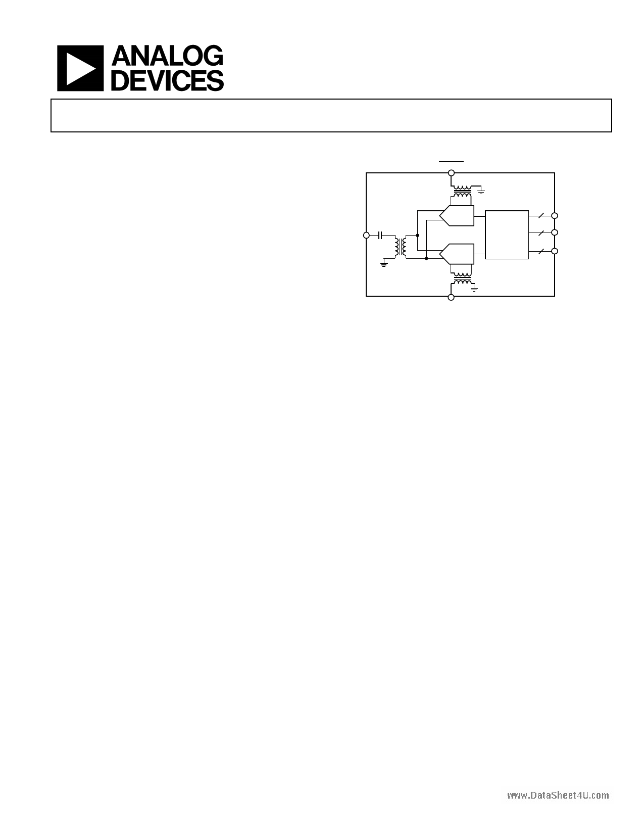
FUNCTIONAL BLOCK DIAGRAM
ENCODE
AD10680
ADC
A
2
OVER RANGE
AIN
DIGITAL
POST
PROCESSING
32
D0 TO D15
ADC
B
2 DATA CLOCK
OUTPUT
ENCODE
Figure 1.
PRODUCT HIGHLIGHTS
1. Guaranteed sample rate up to 100 MSPS.
2. Input signal conditioning with optimized dynamic
performance to 40 MHz.
3. Additional performance options are available, such as
increased SNR performance with digitally selectable input
bandwidths, digitally selectable full-scale input ranges, and
digitally selectable Nyquist zones. Contact sales for more
information.
Rev. PrA
Information furnished by Analog Devices is believed to be accurate and reliable. However, no
responsibility is assumed by Analog Devices for its use, nor for any infringements of patents or other
rights of third parties that may result from its use. Specifications subject to change without notice. No
license is granted by implication or otherwise under any patent or patent rights of Analog Devices.
Trademarksandregisteredtrademarksarethepropertyoftheirrespectiveowners.
One Technology Way, P.O. Box 9106, Norwood, MA 02062-9106, U.S.A.
Tel: 781.329.4700
www.analog.com
Fax: 781.461.3113
©2006 Analog Devices, Inc. All rights reserved.
1 page 
Preliminary Technical Data
PIN CONFIGURATIONS AND FUNCTION DESCRIPTIONS
AD10680www.DataSheet4U.com
AGND 1
2 AGND
3.3V 3
4 AIN
3.3V 5
6 AGND
AGND 7 AD10680 8 AGND
5.0V 9
10 AGND
TOP VIEW
5.0V 11 (Not to Scale) 12 AGND
AGND 13
14 AGND
ENCODE 15
16 AGND
ENCODE 17
18 AGND
AGND 19
20 AGND
Figure 2. Pin Configuration P1
NC 1
2 NC
NC 3
4 NC
DGND 5
6 1.2VD
DCO 7
8 1.2VD
DCO 9
10 1.2VD
DOUT15 (MSB) 11
12 DOUT14
DOUT15 (MSB) 13 AD10680 14 DOUT14
DOUT13 15 TOP VIEW 16 DOUT12
DOUT13 17 (Not to Scale) 18 DOUT12
DOUT11 19
20 DOUT10
DOUT11 21
22 DOUT10
DOUT9 23
24 DOUT8
DOUT9 25
26 DOUT8
NC 27
28 DGND
NC 29
30 DGND
NC = NO CONNECT
Figure 3. Pin Configuration P2
Table 3. Pin Function Descriptions
P1 Pin No.1
P2 Pin No.2
N/A 5, 28, 30
N/A 11 to 26
N/A N/A
N/A N/A
N/A N/A
N/A 6, 8, 10
N/A N/A
N/A N/A
N/A 1 to 4, 27, 29
N/A 7
N/A 9
3, 5 N/A
9, 11 N/A
1, 2, 6, 7, 8, 10, 12,
13, 14, 16, 18, 19, 20
N/A
4 N/A
15 N/A
17 N/A
1 Equivalent pin configuration is J1.
2 Equivalent pin configuration is J2.
3 Equivalent pin configuration is J3.
P3 Pin No.3
18, 20
1 to 16
17
19
23
N/A
22, 24
21
25 to 30
N/A
N/A
N/A
N/A
N/A
N/A
N/A
N/A
Mnemonic
DGND
DOUTx, DOUTx
OR
OR
RESET
1.2VD
2.5VD
3.3VD
NC
DCO
DCO
3.3V
5.0V
AGND
AIN
ENCODE
ENCODE
DOUT7 1
2 DOUT6
DOUT7 3
4 DOUT6
DOUT5 5
6 DOUT4
DOUT5 7
8 DOUT4
DOUT3 9
10 DOUT2
DOUT3 11
12 DOUT2
DOUT1 13 AD10680 14 DOUT0 (LSB)
DOUT1 15 TOP VIEW 16 DOUT0 (LSB)
OR 17 (Not to Scale) 18 DGND
OR 19
20 DGND
3.3VD 21
22 2.5VD
RESET 23
24 2.5VD
NC 25
26 NC
NC 27
28 NC
NC 29
30 NC
Figure 4. Pin Configuration P3
Description
Digital Ground
Data Bit Output, Complement
Overrange
Overrange, Complement
Reset
Digital Voltage
Digital Voltage
Digital Voltage (VDD)
No Connection
Data Clock Output
Data Clock Output, Complement
Encode Voltage (EVCC)
Analog Voltage (AVCC)
Analog Ground
Analog Input
ENCODE Input
ENCODE Input, Complement
Rev. PrA | Page 5 of 8
5 Page | ||
| Páginas | Total 8 Páginas | |
| PDF Descargar | [ Datasheet AD10680.PDF ] | |
Hoja de datos destacado
| Número de pieza | Descripción | Fabricantes |
| AD10680 | 100 MSPS A/D Converter | Analog Devices |
| Número de pieza | Descripción | Fabricantes |
| SLA6805M | High Voltage 3 phase Motor Driver IC. |
Sanken |
| SDC1742 | 12- and 14-Bit Hybrid Synchro / Resolver-to-Digital Converters. |
Analog Devices |
|
DataSheet.es es una pagina web que funciona como un repositorio de manuales o hoja de datos de muchos de los productos más populares, |
| DataSheet.es | 2020 | Privacy Policy | Contacto | Buscar |