|
|
|
PDF 14053B Data sheet ( Hoja de datos )
| Número de pieza | 14053B | |
| Descripción | MC14053B | |
| Fabricantes | ON Semiconductor | |
| Logotipo | ||
Hay una vista previa y un enlace de descarga de 14053B (archivo pdf) en la parte inferior de esta página. Total 12 Páginas | ||
|
No Preview Available !
MC14051B, MC14052B,
MC14053B
www.DataSheet4U.com
Analog
Multiplexers/Demultiplexers
The MC14051B, MC14052B, and MC14053B analog multiplexers
are digitally−controlled analog switches. The MC14051B effectively
implements an SP8T solid state switch, the MC14052B a DP4T, and
the MC14053B a Triple SPDT. All three devices feature low ON
impedance and very low OFF leakage current. Control of analog
signals up to the complete supply voltage range can be achieved.
Features
• Triple Diode Protection on Control Inputs
• Switch Function is Break Before Make
• Supply Voltage Range = 3.0 Vdc to 18 Vdc
• Analog Voltage Range (VDD − VEE) = 3.0 to 18 V
Note: VEE must be v VSS
• Linearized Transfer Characteristics
• Low−noise − 12 nV/√Cycle, f ≥ 1.0 kHz Typical
• Pin−for−Pin Replacement for CD4051, CD4052, and CD4053
• For 4PDT Switch, See MC14551B
• For Lower RON, Use the HC4051, HC4052, or HC4053 High−Speed
CMOS Devices
• Pb−Free Packages are Available*
http://onsemi.com
MARKING
DIAGRAMS
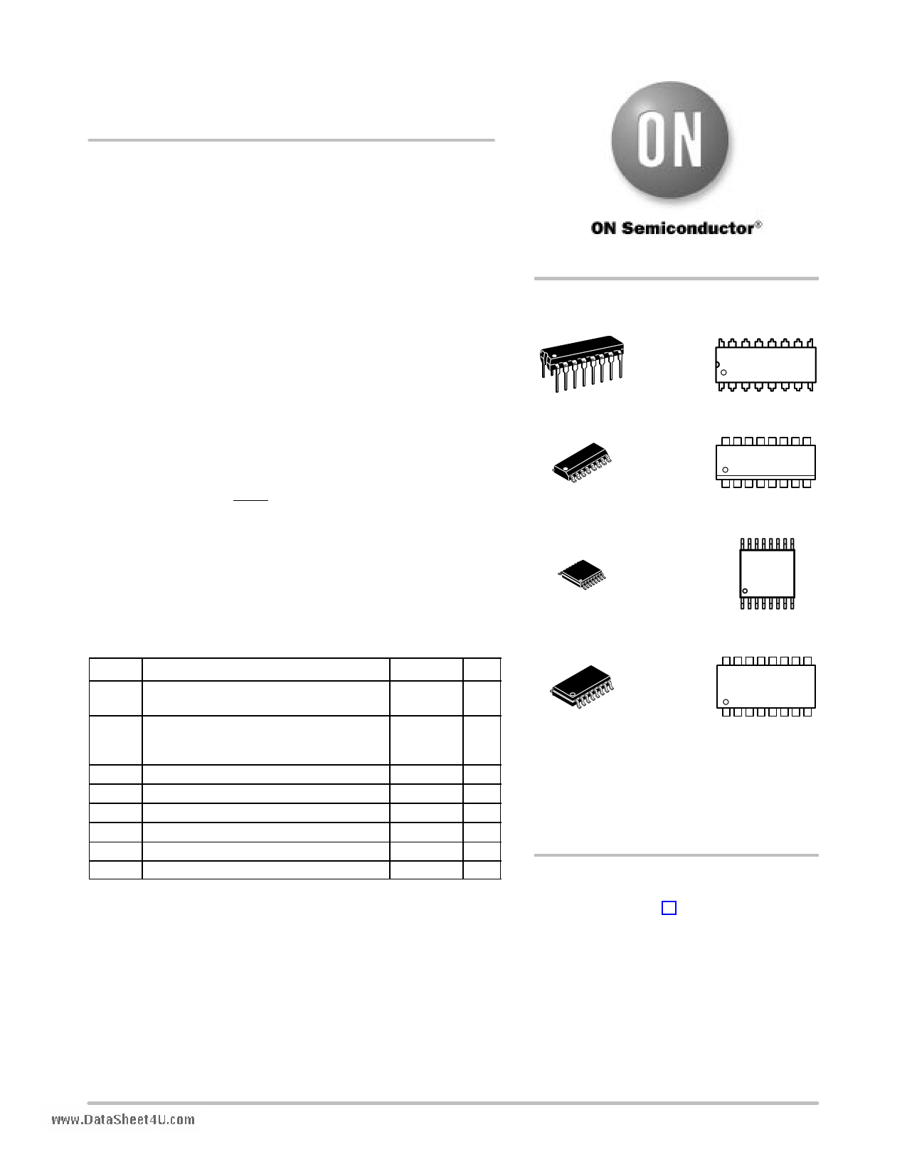
PDIP−16 16
P SUFFIX
CASE 648
1
MC140xxBCP
AWLYYWW
SOIC−16
D SUFFIX
CASE 751B
16
140xxB
AWLYWW
1
TSSOP−16
DT SUFFIX
CASE 948F
16
14
0xxB
ALYW
1
MAXIMUM RATINGS (Voltages Referenced to VSS)
Symbol
Parameter
Value Unit
VDD DC Supply Voltage Range
(Referenced to VEE, VSS ≥ VEE)
−0.5 to
+18.0
V
Vin, Input or Output Voltage Range
−0.5 to VDD V
Vout (DC or Transient) (Referenced to VSS for + 0.5
Control Inputs and VEE for Switch I/O)
Iin Input Current (DC or Transient) per Control Pin
+10
mA
ISW Switch Through Current
± 25 mA
PD Power Dissipation per Package (Note 1)
500 mW
TA Ambient Temperature Range
−55 to +125 °C
Tstg Storage Temperature Range
−65 to +150 °C
TL Lead Temperature (8−Second Soldering)
260 °C
Maximum ratings are those values beyond which device damage can occur.
Maximum ratings applied to the device are individual stress limit values (not
normal operating conditions) and are not valid simultaneously. If these limits are
exceeded, device functional operation is not implied, damage may occur and
reliability may be affected.
1. Temperature Derating: Plastic “P and D/DW” Packages: – 7.0 mW/_C From
65_C To 125_C
This device contains protection circuitry to guard against damage due to high
static voltages or electric fields. However, precautions must be taken to avoid
applications of any voltage higher than maximum rated voltages to this
high−impedance circuit. For proper operation, Vin and Vout should be constrained to
the range VSS v (Vin or Vout) v VDD.
Unused inputs must always be tied to an appropriate logic voltage level (e.g., either
VSS, VEE or VDD). Unused outputs must be left open.
SOEIAJ−16
F SUFFIX
CASE 966
16
MC140xxB
AWLYWW
1
xx
A
WL, L
YY, Y
WW, W
= Specific Device Code
= Assembly Location
= Wafer Lot
= Year
= Work Week
ORDERING INFORMATION
See detailed ordering and shipping information in the package
dimensions section on page 9 of this data sheet.
*For additional information on our Pb−Free strategy
and soldering details, please download the
ON Semiconductor Soldering and Mounting
Techniques Reference Manual, SOLDERRM/D.
© Semiconductor Components Industries, LLC, 2005
February, 2005 − Rev. 6
1
Publication Order Number:
MC14051B/D
1 page 
MC14051B, MC14052B, MC14053B
www.DataSheet4U.com
IN/OUT
VDD VDD VDD
OUT/IN
VEE
LEVEL
CONVERTED
CONTROL
VDD
IN/OUT
OUT/IN
VEE CONTROL
Figure 1. Switch Circuit Schematic
TRUTH TABLE
Control Inputs
Select
ON Switches
Inhibit C* B A MC14051B MC14052B MC14053B
0 0 0 0 X0 Y0 X0 Z0 Y0 X0
0 0 0 1 X1 Y1 X1 Z0 Y0 X1
0 0 1 0 X2 Y2 X2 Z0 Y1 X0
0 0 1 1 X3 Y3 X3 Z0 Y1 X1
0 1 00
0 1 01
0 1 10
0 1 11
X4
X5
X6
X7
Z1 Y0 X0
Z1 Y0 X1
Z1 Y1 X0
Z1 Y1 X1
1 x x x None
*Not applicable for MC14052
x = Don’t Care
None
None
INH 6
A 10
B9
X0 12
X1 14
X2 15
X3 11
Y0 1
Y1 5
Y2 2
Y3 4
16 VDD
LEVEL
CONVERTER
BINARY TO 1−OF−4
DECODER WITH
INHIBIT
8 VSS 7 VEE
13 X
3Y
Figure 3. MC14052B Functional Diagram
INH 6
A 11
B 10
C9
16 VDD
LEVEL
CONVERTER
BINARY TO 1−OF−8
DECODER WITH
INHIBIT
X0 13
X1 14
X2 15
X3 12
X4 1
X5 5
X6 2
X7 4
8 VSS 7 VEE
3X
Figure 2. MC14051B Functional Diagram
INH 6
A 11
B 10
C9
16 VDD
LEVEL
CONVERTER
BINARY TO 1−OF−2
DECODER WITH
INHIBIT
8 VSS 7 VEE
X0 12
X1 13
Y0 2
Y1 1
Z0 5
Z1 3
14 X
15 Y
4Z
Figure 4. MC14053B Functional Diagram
http://onsemi.com
5
5 Page 
MC14051B, MC14052B, MC14053B
PACKAGE DIMENSIONS
TSSOP−16
DT SUFFIX
PLASTIC TSSOP PACKAGE
CASE 948F−01
ISSUE A
www.DataSheet4U.com
0.15 (0.006) T U S
16
2X L/2
L
PIN 1
IDENT.
1
0.15 (0.006) T U S
0.10 (0.004)
−T− SEATING
PLANE
D
C
16X K REF
0.10 (0.004) M T U S V S
9
B
−U− J
8
N
NOTES:
1. DIMENSIONING AND TOLERANCING PER
ANSI Y14.5M, 1982.
2. CONTROLLING DIMENSION: MILLIMETER.
K
K1
ÇÉÇÉÇJ1
ÇÇÉÉÇÇÉÉÇÇSECTION N−N
3. DIMENSION A DOES NOT INCLUDE MOLD
FLASH. PROTRUSIONS OR GATE BURRS.
MOLD FLASH OR GATE BURRS SHALL NOT
EXCEED 0.15 (0.006) PER SIDE.
4. DIMENSION B DOES NOT INCLUDE
INTERLEAD FLASH OR PROTRUSION.
INTERLEAD FLASH OR PROTRUSION SHALL
NOT EXCEED 0.25 (0.010) PER SIDE.
5. DIMENSION K DOES NOT INCLUDE
DAMBAR PROTRUSION. ALLOWABLE
DAMBAR PROTRUSION SHALL BE 0.08
(0.003) TOTAL IN EXCESS OF THE K
DIMENSION AT MAXIMUM MATERIAL
CONDITION.
6. TERMINAL NUMBERS ARE SHOWN FOR
REFERENCE ONLY.
0.25 (0.010)
7. DIMENSION A AND B ARE TO BE
DETERMINED AT DATUM PLANE −W−.
A
−V−
M
N
F
DETAIL E
−W−
MILLIMETERS INCHES
DIM MIN MAX MIN MAX
A 4.90 5.10 0.193 0.200
B 4.30 4.50 0.169 0.177
C −−− 1.20 −−− 0.047
D 0.05 0.15 0.002 0.006
F 0.50 0.75 0.020 0.030
G 0.65 BSC
0.026 BSC
H 0.18 0.28 0.007 0.011
J 0.09 0.20 0.004 0.008
J1 0.09 0.16 0.004 0.006
K 0.19 0.30 0.007 0.012
K1 0.19 0.25 0.007 0.010
L 6.40 BSC
0.252 BSC
M 0_ 8_ 0_ 8_
H DETAIL E
G
http://onsemi.com
11
11 Page | ||
| Páginas | Total 12 Páginas | |
| PDF Descargar | [ Datasheet 14053B.PDF ] | |
Hoja de datos destacado
| Número de pieza | Descripción | Fabricantes |
| 14053B | MC14053B | ON Semiconductor |
| Número de pieza | Descripción | Fabricantes |
| SLA6805M | High Voltage 3 phase Motor Driver IC. |
Sanken |
| SDC1742 | 12- and 14-Bit Hybrid Synchro / Resolver-to-Digital Converters. |
Analog Devices |
|
DataSheet.es es una pagina web que funciona como un repositorio de manuales o hoja de datos de muchos de los productos más populares, |
| DataSheet.es | 2020 | Privacy Policy | Contacto | Buscar |