|
|
|
PDF LF3320 Data sheet ( Hoja de datos )
| Número de pieza | LF3320 | |
| Descripción | Horizontal Digital Image Filter | |
| Fabricantes | LOGIC Devices Incorporated | |
| Logotipo | ||
Hay una vista previa y un enlace de descarga de LF3320 (archivo pdf) en la parte inferior de esta página. Total 24 Páginas | ||
|
No Preview Available !
DEVICES INCORPORATED
DEVICES INCORPORATED
LF3320
LF3320Horizontal Digital Image Filter
Horizontal Digital Image Filter
FEATURES
DESCRIPTION
❑ 83 MHz Data Rate
❑ 12-bit Data or Coefficients (Expand-
able to 24-bit)
❑ 32-Tap FIR Filter, Cascadable for
More Filter Taps
❑ Over 49 K-bits of on-board Memory
❑ LF InterfaceTM Allows All 256
Coefficient Sets to be Updated
Within Vertical Blanking
❑ Various Operating Modes: Dual
Filter, Single Filter, Double Wide
Data or Coefficient, Matrix Multipli-
cation, and Accumulator Access.
❑ Selectable 16-bit Data Output with
User-Defined Rounding and Limiting
❑ Supports Interleaved Data Streams
❑ Supports Decimation up to 16:1 for
Increasing Number of Filter Taps
❑ 3.3 Volt Supply
❑ 144 Lead PQFP
The LF3320 filters digital images in the
horizontal dimension at real-time
video rates. The input and coefficient
data are both 12 bits and in two’s
complement format. The output is also
in two’s complement format and may
be rounded to 16 bits.
The LF3320 is designed to take
advantage of symmetric coefficient
sets. When symmetric coefficient sets
are used, the device can be configured
as a single 32-tap FIR filter or as two
separate 16-tap FIR filters.
When asymmetric coefficient sets are
used, the device can be configured as a
single 16-tap FIR filter or as two
separate 8-tap FIR filters. Multiple
LF3320s can be cascaded to create
larger filters.
Interleave/Decimation Registers (I/D
Registers) allow interleaved data to be
fed directly into the device and filtered
without separating the data into
individual data streams.
The LF3320 can handle a maximum of
sixteen data sets interleaved together.
The I/D Registers and on-chip accu-
mulators facilitate using decimation to
increase the number of filter taps.
Decimation of up to 16:1 is supported.
The LF3320 contains enough on-board
memory to store 256 coefficient sets.
Two separate LF InterfacesTM allow all
256 coefficient sets to be updated within
vertical blanking.
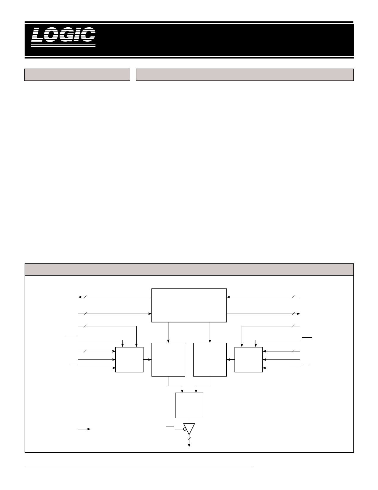
LF3320 BLOCK DIAGRAM
12
ROUT11-0
12
DIN11-0
8
CAA7-0
CENA
12
CFA11-0
PAUSEA
LDA
INTERLEAVE / DECIMATION
REGISTERS
256
COEFFICIENT
SET
STORAGE
16-TAP
FILTER A
16-TAP
FILTER B
256
COEFFICIENT
SET
STORAGE
12
RIN11-0
12
COUT11-0
8
CAB7-0
CENB
12
CFB11-0
PAUSEB
LDB
ROUND
SELECT
LIMIT
CIRCUITRY
CLK
OED
16
DOUT15-0
Video Imaging Products
2-1 08/16/2000–LDS.3320-N
1 page 
DEVICES INCORPORATED
LF3320
Horizontal Digital Image Filter
Registers on the rising edge of CLK.
When SHENB is HIGH, data can not be
loaded into the Cascade Registers or
shifted through the I/D Registers and
their contents will not be changed.
In Single Filter Mode, SHENB also
enables or disables the loading of data
into the Input (DIN11-0), Reverse
Cascade Output (ROUT11-0) and Filter
A I/D Registers. It is important to note
that in Single Filter Mode, both
SHENA and SHENB should be
connected together. Both must be
active to enable data loading in Single
Filter Mode. SHENB is latched on the
rising edge of CLK.
ROUT3-0 are enabled for output. When
OEC is HIGH, COUT11-0 and ROUT3-0
are placed in a high-impedance state.
PAUSEA — LF InterfaceTM Pause
When PAUSEA is HIGH, the Filter A
LF InterfaceTM loading sequence is
halted until PAUSEA is returned to a
LOW state. This effectively allows the
user to load coefficients and control
registers at a slower rate than the
master clock (see the LF InterfaceTM
section for a full discussion).
FIGURE 4. SINGLE FILTER MODE
PAUSEB — LF InterfaceTM Pause
When PAUSEB is HIGH, the Filter B LF
InterfaceTM loading sequence is halted
until PAUSEB is returned to a LOW
state. This effectively allows the user
to load coefficients and control regis-
ters at a slower rate than the master
clock (see the LF InterfaceTM section for
a full discussion).
RSLA3-0 — Filter A Round/Select/Limit
Control
ROUT11-0
DIN11-0
12
12
I/D
REGISTERS
I/D
REGISTERS
12
RIN11-0
12
COUT11-0
RSLA3-0 determines which of the
sixteen user-programmable Round/
Select/Limit registers (RSL registers)
are used in the Filter A RSL circuitry.
A value of 0 on RSLA3-0 selects RSL
register 0. A value of 1 selects RSL
register 1 and so on. RSLA3-0 is
latched on the rising edge of CLK (see
the round, select, and limit sections for
a complete discussion).
RSLB3-0 — Filter B Round/Select/Limit
Control
FILTER
A
FILTER
B
RSL
CIRCUIT
16
DOUT15-0
RSLB3-0 determines which of the sixteen
user-programmable RSL registers are
used in the Filter B RSL circuitry. A
value of 0 on RSLB3-0 selects RSL
register 0. A value of 1 selects RSL
register 1 and so on. RSLB3-0 is latched
on the rising edge of CLK (see the round,
select, and limit sections for a complete
discussion).
FIGURE 5. DUAL FILTER MODE
12
DIN11-0
I/D
REGISTERS
FILTER
A
I/D
REGISTERS
FILTER
B
12
RIN11-0
OED — DOUT Output Enable
When OED is LOW, DOUT15-0 is
enabled for output. When OED is
HIGH, DOUT15-0 is placed in a high-
impedance state.
OEC— COUT/ROUT Output Enable
When OEC is LOW, COUT11-0 and
R.S.L.
CIRCUIT
16
DOUT15-0
R.S.L.
CIRCUIT
16
ROUT3-0 / COUT11-0
Video Imaging Products
2-5 08/16/2000–LDS.3320-N
5 Page 
DEVICES INCORPORATED
LF3320
Horizontal Digital Image Filter
TABLE 2. CONFIGURATION REGISTER 0 – ADDRESS 200H
BITS FUNCTION
DESCRIPTION
0 ALU Mode Filter A
0: A + B
1: B – A
1 Pass A Filter A
0 : ALU Input A = 0
1 : ALU Input A = Forward Register Path
2 Pass B Filter A
0 : ALU Input B = 0
1 : ALU Input B = Reverse Register Path
11-3 Reserved
Should be set to “0”
TABLE 3. CONFIGURATION REGISTER 1 – ADDRESS 201H
BITS FUNCTION
DESCRIPTION
0 Filter A Odd-Tap
Interleave Mode
0 : Odd-Tap Interleave Mode Disabled
1 : Odd-Tap Interleave Mode Enabled
4-1 Filter A I/D Register Length 0000 :
0001 :
0010 :
0011 :
0100 :
0101 :
0110 :
0111 :
1000 :
1001 :
1010 :
1011 :
1100 :
1101 :
1110 :
1111 :
1 Register
2 Registers
3 Registers
4 Registers
5 Registers
6 Registers
7 Registers
8 Registers
9 Registers
1 0 Registers
1 1 Registers
1 2 Registers
1 3 Registers
1 4 Registers
1 5 Registers
1 6 Registers
5 Filter A Tap Number
0 : Even Number of Taps
1 : Odd Number of Taps
6 Filter A Data Reversal
0 : Data Reversal Enabled
1 : Data Reversal Disabled
11-7 Reserved
Should be set to “0”
I/D Register Data Path Control
The three multiplexers in the I/D
Register data path control how data
is routed through the forward and
reverse data paths.
The forward data path contains the
I/D Registers in which data flows
from left to right in the block diagram
in Figure 1. The reverse data path
contains the I/D Registers in which
data flows from right to left.
In Single or Dual Filter Modes, data
is fed from the forward data path to
the reverse data path as follows.
When the filter is configured for an
even number of taps, data from the
last I/D Register in the forward data
path is fed into the first I/D Register
in the reverse data path (see Figure 13).
When the filter is configured for an
odd number of taps, the data which
will appear at the output of the last
I/D Register in the forward data
path on the next clock cycle is fed
into the first I/D Register in the
reverse data path. Bit 5 in Configu-
ration Register 1 and Configuration
Register 3 configures Filters A and B
respectively for an even or odd
number of taps.
When interleaved data is fed through
the device and an even tap filter is
desired, the filter should be configured
for an even number of taps and the I/D
Register length should match the
number of data sets interleaved together.
When interleaved data is fed through
the device and an odd tap filter is
desired, the filter should be set to
Odd-Tap Interleave Mode. Bit 0 of
Configuration Register 1 and Configura-
tion Register 3 configures Filters A and
B respectively for Odd-Tap Interleave
Mode. When the filter is configured for
Odd-Tap Interleave Mode, data from the
next to last I/D Register in the forward
data path is fed into the first I/D
Register in the reverse data path.
When the filter is configured for an odd
number of taps (interleaved or
non-interleaved modes), the filter is
structured such that the center data
value is aligned simultaneously at the A
and B inputs of the last ALU in the
forward data path. In order to achieve
the correct result, the user must divide
the coefficient by two.
Data Reversal
Data reversal circuitry is placed after the
multiplexers which route data from the
forward data path to the reverse data
path (see Figure 14). When decimating,
the data stream must be reversed in
order for data to be properly aligned at
the inputs of the ALUs.
When data reversal is enabled, the
circuitry uses a pair of LIFOs to reverse
the order of the data sent to the reverse
data path. TXFRA and TXFRB control
the LIFOs in Filters A and B respectively.
When TXFRA/TXFRB goes LOW, the
LIFO sending data to the reverse data
path becomes the LIFO receiving data
from the forward data path,andtheLIFO
receivingdatafrom the forward data
path becomes the LIFO sending data to
Video Imaging Products
2-11
08/16/2000–LDS.3320-N
11 Page | ||
| Páginas | Total 24 Páginas | |
| PDF Descargar | [ Datasheet LF3320.PDF ] | |
Hoja de datos destacado
| Número de pieza | Descripción | Fabricantes |
| LF3320 | Horizontal Digital Image Filter | LOGIC Devices Incorporated |
| LF3321 | Horizontal Digital Image Filter | LOGIC Devices |
| LF3324 | 24Mbit Frame Buffer/FIFO | LOGIC DEVICES |
| Número de pieza | Descripción | Fabricantes |
| SLA6805M | High Voltage 3 phase Motor Driver IC. |
Sanken |
| SDC1742 | 12- and 14-Bit Hybrid Synchro / Resolver-to-Digital Converters. |
Analog Devices |
|
DataSheet.es es una pagina web que funciona como un repositorio de manuales o hoja de datos de muchos de los productos más populares, |
| DataSheet.es | 2020 | Privacy Policy | Contacto | Buscar |