|
|
PDF ADC11DV200 Data sheet ( Hoja de datos )
| Número de pieza | ADC11DV200 | |
| Descripción | 200 MSPS Low-Power A/D Converter | |
| Fabricantes | National Semiconductor Corporation | |
| Logotipo | ||
Hay una vista previa y un enlace de descarga de ADC11DV200 (archivo pdf) en la parte inferior de esta página. Total 24 Páginas | ||
|
No Preview Available !
www.DataSheet4U.com
ADC11DV200
April 23, 2009
Dual 11-bit, 200 MSPS Low-Power A/D Converter with
Parallel LVDS/CMOS Outputs
General Description
The ADC11DV200 is a monolithic analog-to-digital converter
capable of converting two analog input signals into 11-bit dig-
ital words at rates up to 200 Mega Samples Per Second
(MSPS). The digital output mode is selectable and can be ei-
ther differential LVDS or CMOS signals. This converter uses
a differential, pipelined architecture with digital error correc-
tion and an on-chip sample-and-hold circuit to minimize die
size and power consumption while providing excellent dy-
namic performance. A unique sample-and-hold stage yields
a full-power bandwidth of 900MHz. Fabricated in core CMOS
process, the ADC11DV200 may be operated from a single
1.8V power supply. The ADC11DV200 achieves approxi-
mately 10.06 effective bits at Nyquist and consumes just
280mW at 170MSPS in CMOS mode 450mW at 200MSPS in
LVDS mode. The power consumption can be scaled down
further by reducing sampling rates.
Applications
■ Digital Predistortion (DPD)
■ Wireless Communications Infrastructure
■ Medical Imaging
■ Portable Instrumentation
■ Digital Video
Features
■ Single 1.8V power supply operation.
■ Power scaling with clock frequency.
■ Internal sample-and-hold.
■ Internal or external reference.
■ Power down mode.
■ Offset binary or 2's complement output data format.
■ LVDS or CMOS output signals.
■ 60-pin LLP package, (9x9x0.8mm, 0.5mm pin-pitch)
■ Clock Duty Cycle Stabilizer.
■ IF Sampling Bandwidth > 900MHz.
Key Specifications
■ Resolution
11 Bits
■ Conversion Rate
200 MSPS
■ ENOB
10.06 bits (typ) @Fin=70MHz
■ SNR
62.5 dBFS (typ) @Fin=70MHz
■ SINAD
62.3 dBFS (typ) @Fin=70MHz
■ SFDR
82 dBFS (typ) @Fin=70MHz
■ LVDS Power
450 mW (typ) @Fs=200 MSPS
■ CMOS Power
280 mW (typ) @Fs=170 MSPS
■ Operating Temp. Range
−40°C to +85°C.
Block Diagram
© 2009 National Semiconductor Corporation 300875
30087502
www.national.com
1 page 
Pin No.
Symbol
CwMwOwS.DOauttapSuthMeoedt4eU.com
24-29,
32-35,51
DA0-DA10
39-44,
47-50,52
DB0-DB10
37 DRDYA
38 DRDYB
ANALOG POWER
8, 16, 18, 59,
60
VA
1, 4, 12, 15,
22, 55, 58, EP
DIGITAL POWER
AGND
21, 54
VD
31, 45
30, 46
VDR
DRGND
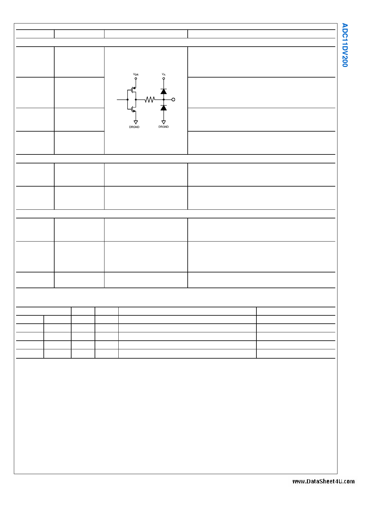
Equivalent Circuit
Description
Digital data output pins that make up the 11-bit conversion
result for Channel A. DA0 (pin 24) is the LSB, while DA10 (pin
51) is the MSB of the output word. Output levels are CMOS
compatible.
Digital data output pins that make up the 11-bit conversion
result for Channel B. DB0 (pin 39) is the LSB, while DB10 (pin
52) is the MSB of the output word. Output levels are CMOS
compatible.
Data Ready Strobe for channel A. This signal is used to clock
the A-Channel output data. DRDYA is a SDR clock with same
frequency as CLK rate and data is valid on the rising edges.
Data Ready Strobe for channel B. This signal is used to clock
the B-Channel output data. DRDYB is a SDR clock with same
frequency as CLK rate and data is valid on the rising edges.
Positive analog supply pins. These pins should be connected
to a quiet source and be bypassed to AGND with 0.1 µF
capacitors located close to the power pins.
The ground return for the analog supply.
Exposed Pad (EP) must be soldered to AGND to ensure rated
performance.
Positive digital supply pins. These pins should be connected
to a quiet source and be bypassed to AGND with 0.1 µF
capacitors located close to the power pins.
Positive driver supply pin for the output drivers. This pin should
be connected to a quiet voltage source and be bypassed to
DRGND with a 0.1 µF capacitor located close to the power
pin.
The ground return for the digital output driver supply. This pin
should be connected to the system digital ground.
Voltage on DF/DCS
Min Max
0 mV 200mV
250 mV 600 mV
750 mV 1250 mV
1400mV
VA
TABLE 1. Voltage on DF/DCS Pin and Corresponding Chip Response
Results
DF DCS
1 1 2's complement data, duty cycle correction on
0 0 Offset binary data, duty cycle correction off
1 0 2's complement data, duty cycle correction off
0 1 Offset binary data, duty cycle correction on
Suggestions
Tie to AGND
Leave floating
Tie to VA
5 www.national.com
5 Page 
Timing Diagrams
www.DataSheet4U.com
FIGURE 1. LVDS Output Timing
30087509
FIGURE 2. CMOS Output Timing
11
30087516
www.national.com
11 Page | ||
| Páginas | Total 24 Páginas | |
| PDF Descargar | [ Datasheet ADC11DV200.PDF ] | |
Hoja de datos destacado
| Número de pieza | Descripción | Fabricantes |
| ADC11DV200 | 200 MSPS Low-Power A/D Converter | National Semiconductor Corporation |
| ADC11DV200 | Dual 11-bit 200 MSPS Low-Power A/D Converter with Parallel LVDS/CMOS Outputs (Rev. A) | Texas Instruments |
| Número de pieza | Descripción | Fabricantes |
| SLA6805M | High Voltage 3 phase Motor Driver IC. |
Sanken |
| SDC1742 | 12- and 14-Bit Hybrid Synchro / Resolver-to-Digital Converters. |
Analog Devices |
|
DataSheet.es es una pagina web que funciona como un repositorio de manuales o hoja de datos de muchos de los productos más populares, |
| DataSheet.es | 2020 | Privacy Policy | Contacto | Buscar |
