|
|
|
PDF AD9601 Data sheet ( Hoja de datos )
| Número de pieza | AD9601 | |
| Descripción | 200 MSPS/250 MSPS 1.8 V Analog-to-Digital Converter | |
| Fabricantes | Analog Devices | |
| Logotipo | ||
Hay una vista previa y un enlace de descarga de AD9601 (archivo pdf) en la parte inferior de esta página. Total 30 Páginas | ||
|
No Preview Available !
www.daFtaEsAhTeeUt4RuE.cSom
SNR = 59.4 dBFS @ fIN up to 70 MHz @ 250 MSPS
ENOB of 9.7 @ fIN up to 70 MHz @ 250 MSPS (−1.0 dBFS)
SFDR = 81 dBc @ fIN up to 70 MHz @ 250 MSPS (−1.0 dBFS)
Excellent linearity
DNL = 0.2 LSB typical
INL = 0.2 LSB typical
CMOS outputs
Single data port at up to 250 MHz
Demultiplexed dual port at up to 2 × 125 MHz
700 MHz full power analog bandwidth
On-chip reference, no external decoupling required
Integrated input buffer and track-and-hold
Low power dissipation
274 mW @ 200 MSPS
322 mW @ 250 MSPS
Programmable input voltage range
1.0 V to 1.5 V, 1.25 V nominal
1.8 V analog and digital supply operation
Selectable output data format (offset binary, twos
complement, Gray code)
Clock duty cycle stabilizer
Integrated data capture clock
10-Bit, 200 MSPS/250 MSPS
1.8 V Analog-to-Digital Converter
AD9601
APPLICATIONS
Wireless and wired broadband communications
Cable reverse path
Communications test equipment
Radar and satellite subsystems
Power amplifier linearization
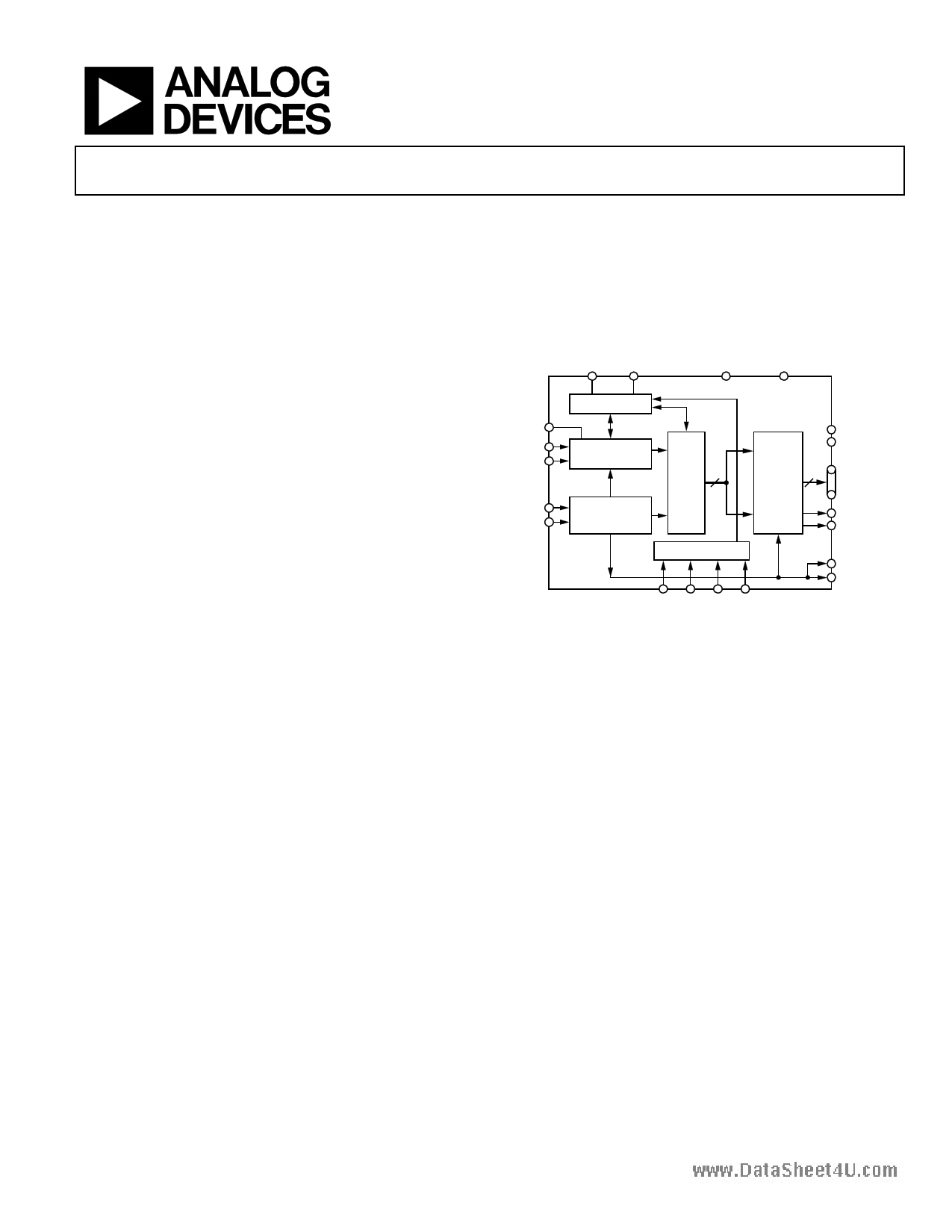
FUNCTIONAL BLOCK DIAGRAM
RBIAS PWDN
AGND
AVDD (1.8V)
CML
VIN+
VIN–
CLK+
CLK–
REFERENCE
AD9601
TRACK-AND-HOLD
CLOCK
MANAGEMENT
ADC 10
10-BIT
CORE
SERIAL PORT
OUTPUT 10
STAGING
LVDS
RESET SCLK SDIO CSB
Figure 1.
DRVDD
DRGND
Dx9 TO Dx0
OVRA
OVRB
DCO+
DCO–
GENERAL DESCRIPTION
The AD9601 is a 10-bit monolithic sampling analog-to-digital
converter optimized for high performance, low power, and ease
of use. The product operates at up to a 250 MSPS conversion
rate and is optimized for outstanding dynamic performance in
wideband carrier and broadband systems. All necessary func-
tions, including a track-and-hold (T/H) and voltage reference,
are included on the chip to provide a complete signal
conversion solution.
The ADC requires a 1.8 V analog voltage supply and a differen-
tial clock for full performance operation. The digital outputs are
CMOS compatible and support either twos complement, offset
binary format, or Gray code. A data clock output is available for
proper output data timing.
Fabricated on an advanced CMOS process, the AD9601 is
available in a 56-lead LFCSP, specified over the industrial
temperature range (−40°C to +85°C).
PRODUCT HIGHLIGHTS
1. High Performance—Maintains 59.4 dBFS SNR @ 250 MSPS
with a 70 MHz input.
2. Low Power—Consumes only 322 mW @ 250 MSPS.
3. Ease of Use—CMOS output data and output clock signal
allow interface to current FPGA technology. The on-chip
reference and sample-and-hold provide flexibility in
system design. Use of a single 1.8 V supply simplifies
system power supply design.
4. Serial Port Control—Standard serial port interface supports
various product functions, such as data formatting, power-
down, gain adjust, and output test pattern generation.
5. Pin-Compatible Family—12-bit pin-compatible family
offered as the AD9626.
Rev. 0
Information furnished by Analog Devices is believed to be accurate and reliable. However, no
responsibility is assumed by Analog Devices for its use, nor for any infringements of patents or other
rights of third parties that may result from its use. Specifications subject to change without notice. No
license is granted by implication or otherwise under any patent or patent rights of Analog Devices.
Trademarksandregisteredtrademarksarethepropertyoftheirrespectiveowners.
One Technology Way, P.O. Box 9106, Norwood, MA 02062-9106, U.S.A.
Tel: 781.329.4700
www.analog.com
Fax: 781.461.3113
©2007 Analog Devices, Inc. All rights reserved.
1 page 
AD9601
DIGITAL SPECIFICATIONS
AVDD = 1.8 V, DRVDD = 1.8 V, TMIN = −40°C, TMAX = +85°C, fIN = −1.0 dBFS, full scale = 1.25 V, DCS enabled, unless otherwise noted.
Table 3.
www.daPtaarsahmeeet4teur.c1om
CLOCK INPUTS
Logic Compliance
Internal Common-Mode Bias
Differential Input Voltage
Input Voltage Range
Input Common-Mode Range
High Level Input Voltage (VIH)
Low Level Input Voltage (VIL)
Input Resistance (Differential)
Input Capacitance
LOGIC INPUTS
Logic 1 Voltage
Logic 0 Voltage
Logic 1 Input Current (SDIO)
Logic 0 Input Current (SDIO)
Logic 1 Input Current
(SCLK, PDWN, CSB, RESET)
Logic 0 Input Current
(SCLK, PDWN, CSB, RESET)
Input Capacitance
LOGIC OUTPUTS
High Level Output Voltage
Low Level Output Voltage
Output Coding
Temp Min
AD9601-200
Typ Max
AD9601-250
Min Typ Max
Unit
Full CMOS/LVDS/LVPECL
CMOS/LVDS/LVPECL
Full 1.2
1.2 V
Full 0.2
6 0.2
6 V p-p
Full AVDD − 0.3
AVDD + 1.6 AVDD − 0.3
AVDD + 1.6 V
Full 1.1
AVDD
1.1
AVDD
V
Full 1.2
3.6 1.2
3.6 V
Full 0
0.8 0
0.8 V
Full 16
20 24
16
20 24
kΩ
Full 4
4 pF
Full 0.8 × VDD
Full
Full
Full
Full
Full
25°C
0.2 × AVDD
0
−60
55
0
4
0.8 × VDD
0.2 × AVDD
0
−60
50
0
4
V
V
μA
μA
μA
μA
pF
Full DRVDD − 0.05
DRVDD − 0.05
Full GND + 0.05
GND + 0.05
Twos complement, Gray code, or offset binary (default)
V
V
1 See the AN-835 Application Note, Understanding High Speed ADC Testing and Evaluation, for a complete set of definitions and how these tests were completed.
Rev. 0 | Page 5 of 32
5 Page 
EQUIVALENT CIRCUITS
AVDD
www.datasheet4u.com
CLK+
1.2V
10kΩ
10kΩ
CLK–
Figure 5. Clock Inputs
AVDD
VIN+
VIN–
AVDD
BUF
2kΩ
BUF
2kΩ
BUF
AVDD
VCML
~1.4V
Figure 6. Analog Inputs (VCML = ~1.4 V)
SCLK/DFS
RESET
PDWN
1kΩ
30kΩ
Figure 7. Equivalent SCLK/DFS, RESET, PDWN Input Circuit
CSB
AVDD
26kΩ 1kΩ
AD9601
Figure 8. Equivalent CSB Input Circuit
DRVDD
DRGND
Figure 9. CMOS Outputs (Dx, OVRA, OVRB, DCO+, DCO−)
DRVDD
SDIO/DCS
1kΩ
Figure 10. Equivalent SDIO/DCS Input Circuit
Rev. 0 | Page 11 of 32
11 Page | ||
| Páginas | Total 30 Páginas | |
| PDF Descargar | [ Datasheet AD9601.PDF ] | |
Hoja de datos destacado
| Número de pieza | Descripción | Fabricantes |
| AD9600 | 1.8 V Dual Analog-to-Digital Converter | Analog Devices |
| AD9601 | 200 MSPS/250 MSPS 1.8 V Analog-to-Digital Converter | Analog Devices |
| AD9608 | 1.8V Dual Analog-to-Digital Converter | Analog Devices |
| AD9609 | 1.8V Analog-to-Digital Converter | Analog Devices |
| Número de pieza | Descripción | Fabricantes |
| SLA6805M | High Voltage 3 phase Motor Driver IC. |
Sanken |
| SDC1742 | 12- and 14-Bit Hybrid Synchro / Resolver-to-Digital Converters. |
Analog Devices |
|
DataSheet.es es una pagina web que funciona como un repositorio de manuales o hoja de datos de muchos de los productos más populares, |
| DataSheet.es | 2020 | Privacy Policy | Contacto | Buscar |