|
|
|
PDF C8051F042 Data sheet ( Hoja de datos )
| Número de pieza | C8051F042 | |
| Descripción | (C8051F040 - C8051F043) Mixed-Signal MCU | |
| Fabricantes | Cygnal | |
| Logotipo | ||
Hay una vista previa y un enlace de descarga de C8051F042 (archivo pdf) en la parte inferior de esta página. Total 30 Páginas | ||
|
No Preview Available !
PRELIMINARY
C8051F040/1/2/3
Mixed-Signal ISP FLASH MCU Family
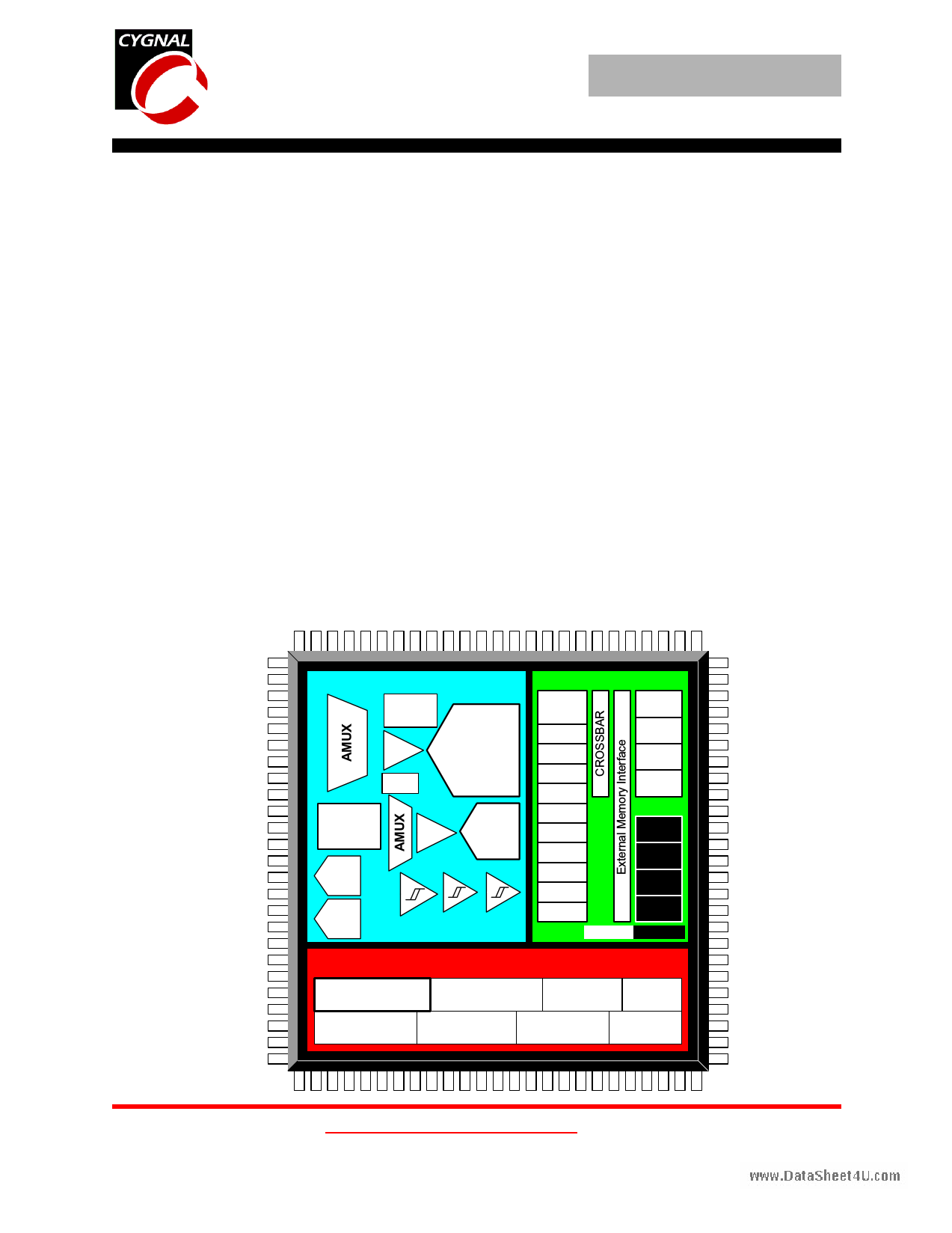
ANALOG PERIPHERALS
- 10 or 12-Bit SAR ADC
• 12-Bit (C8051F040/1) or 10-bit (C8051F042/3) Resolution
• ± 1 LSB INL, guaranteed no missing codes
• Programmable Throughput up to 100 ksps
• 13 External Inputs; Single-Ended or Differential
• SW Programmable High Voltage Difference Amplifier
• Programmable Amplifier Gain: 16, 8, 4, 2, 1, 0.5
• Data-Dependent Windowed Interrupt Generator
• Built-in Temperature Sensor
- 8-bit SAR ADC
• Programmable Throughput up to 500 ksps
www.DataSheet4U.com • 8 External Inputs, Single-ended or differential
• Programmable Amplifier Gain: 4, 2, 1, 0.5
- Two 12-bit DACs
• Can Synchronize Outputs to Timers for Jitter-Free Wave-
form Generation
- Three Analog Comparators
• Programmable Hysteresis/Response Time
- Voltage Reference
- Precision VDD Monitor/Brown-Out Detector
ON-CHIP JTAG DEBUG & BOUNDARY SCAN
- On-Chip Debug Circuitry Facilitates Full- Speed, Non-
Intrusive In-Circuit/In-System Debugging
- Provides Breakpoints, Single-Stepping, Watchpoints,
Stack Monitor; Inspect/Modify Memory and Registers
- Superior Performance to Emulation Systems Using ICE-
Chips, Target Pods, and Sockets
- IEEE1149.1 Compliant Boundary Scan
- Complete Development Kit
HIGH SPEED 8051 µC CORE
- Pipelined Instruction Architecture; Executes 70% of
Instruction Set in 1 or 2 System Clocks
- Up to 25 MIPS Throughput with 25 MHz Clock
- 20 Vectored Interrupt Sources
MEMORY
- 4352 Bytes Internal Data RAM (4k + 256)
- 64k Bytes FLASH; In-System programmable in 512-byte
Sectors
- External 64k Byte Data Memory Interface (programma-
ble multiplexed or non-multiplexed modes)
DIGITAL PERIPHERALS
- 8 Byte-Wide Port I/O (C8051F040/2); 5V tolerant
- 4 Byte-Wide Port I/O (C8051F041/3); 5V tolerant
- Bosch Controller Area Network (CAN 2.0B), Hardware
SMBus™ (I2C™ Compatible), SPI™, and Two UART
Serial Ports Available Concurrently
- Programmable 16-bit Counter/Timer Array with
6 Capture/Compare Modules
- 5 General Purpose 16-bit Counter/Timers
- Dedicated Watch-Dog Timer; Bi-directional Reset Pin
CLOCK SOURCES
- Internal Calibrated Programmable Oscillator: 3 to
24.5 MHz
- External Oscillator: Crystal, RC, C, or Clock
- Real-Time Clock Mode using Timer 2, 3, 4, or PCA
SUPPLY VOLTAGE .......................... 2.7V TO 3.6V
- Multiple Power Saving Sleep and Shutdown Modes
100-Pin TQFP and 64-Pin TQFP Packages Available
Temperature Range: -40°C to +85°C
ANALOG PERIPHERALS
TEMP
SENSOR
PGA
VREF
10/12-bit
100ksps
ADC
HV
DIFF AMP
12-Bit
DAC
12-Bit
DAC
8-bit
PGA 500ksps
ADC
+++
---
VOLTAGE
COMPARATORS
DIGITAL I/O
CAN
2.0B
UART0
Port 0
Port 1
UART1
SMBus
SPI Bus
Port 2
Port 3
PCA
Timer 0
Port 4
Timer 1
Timer 2
Timer 3
Timer 4
Port 5
Port 6
Port 7
64 pin 100 pin
HIGH-SPEED CONTROLLER CORE
8051 CPU
(25MIPS)
20
INTERRUPTS
64KB
ISP FLASH
DEBUG
CIRCUITRY
4352 B
SRAM
JTAG
CLOCK
SANITY
CIRCUIT CONTROL
DS005-1.2MAY03
CYGNAL Integrated Products, Inc. © 2003
Page 1
1 page 
PRELIMINARY
C8051F040/1/2/3
13.7.4. Setting WDT Interval...........................................................................................158
14. OSCILLATORS...................................................................................................................161
14.1.Programmable Internal Oscillator .................................................................................161
14.2.External Oscillator Drive Circuit...................................................................................163
14.3.System Clock Selection.................................................................................................163
14.4.External Crystal Example..............................................................................................165
14.5.External RC Example ....................................................................................................165
14.6.External Capacitor Example..........................................................................................165
15. FLASH MEMORY ..............................................................................................................167
15.1.Programming The Flash Memory .................................................................................167
www.DataSheet4U.com 15.2. Non-volatile Data Storage .............................................................................................168
15.3.Security Options ............................................................................................................168
16. EXTERNAL DATA MEMORY INTERFACE AND ON-CHIP XRAM.......................173
16.1.Accessing XRAM..........................................................................................................173
16.1.1. 16-Bit MOVX Example.......................................................................................173
16.1.2. 8-Bit MOVX Example.........................................................................................173
16.2.Configuring the External Memory Interface .................................................................174
16.3.Port Selection and Configuration ..................................................................................174
16.4.Multiplexed and Non-multiplexed Selection.................................................................176
16.4.1. Multiplexed Configuration ..................................................................................176
16.4.2. Non-multiplexed Configuration...........................................................................177
16.5.Memory Mode Selection ...............................................................................................178
16.5.1. Internal XRAM Only ...........................................................................................178
16.5.2. Split Mode without Bank Select ..........................................................................178
16.5.3. Split Mode with Bank Select ...............................................................................179
16.5.4. External Only .......................................................................................................179
16.6.Timing .......................................................................................................................179
16.6.1. Non-multiplexed Mode........................................................................................181
16.6.1.1.16-bit MOVX: EMI0CF[4:2] = ‘101’, ‘110’, or ‘111’................................181
16.6.1.2. 8-bit MOVX without Bank Select: EMI0CF[4:2] = ‘101’ or ‘111’............182
16.6.1.3. 8-bit MOVX with Bank Select: EMI0CF[4:2] = ‘110’. ..............................183
16.6.2. Multiplexed Mode................................................................................................184
16.6.2.1.16-bit MOVX: EMI0CF[4:2] = ‘001’, ‘010’, or ‘011’................................184
16.6.2.2. 8-bit MOVX without Bank Select: EMI0CF[4:2] = ‘001’ or ‘011’............185
16.6.2.3. 8-bit MOVX with Bank Select: EMI0CF[4:2] = ‘010’. ..............................186
17. PORT INPUT/OUTPUT .....................................................................................................189
17.1.Ports 0 through 3 and the Priority Crossbar Decoder....................................................190
17.1.1. Crossbar Pin Assignment and Allocation ............................................................191
17.1.2. Configuring the Output Modes of the Port Pins ..................................................192
17.1.3. Configuring Port Pins as Digital Inputs ...............................................................193
17.1.4. Weak Pull-ups......................................................................................................193
17.1.5. Configuring Port 1, 2, and 3 Pins as Analog Inputs ............................................193
17.1.6. External Memory Interface Pin Assignments ......................................................194
17.1.7. Crossbar Pin Assignment Example......................................................................197
17.2.Ports 4 through 7 (C8051F040/F042 only) ...................................................................208
© 2003 Cygnal Integrated Products, Inc. DS005-1.2MAY03
Page 3
5 Page 
PRELIMINARY
C8051F040/1/2/3
Figure 7.9. ADC2 Data Word Example.................................................................................93
Figure 7.10. ADC2GT: ADC2 Greater-Than Data Register ...................................................94
Figure 7.11. ADC2LT: ADC2 Less-Than Data Register ........................................................94
Figure 7.12. ADC Window Compare Examples, Single-Ended Mode ...................................95
Figure 7.13. ADC Window Compare Examples, Differential Mode ......................................96
Table 7.1. ADC2 Electrical Characteristics..........................................................................97
8. DACS, 12-BIT VOLTAGE MODE ......................................................................................99
Figure 8.1. DAC Functional Block Diagram .........................................................................99
Figure 8.2. DAC0H: DAC0 High Byte Register .................................................................101
Figure 8.3. DAC0L: DAC0 Low Byte Register ..................................................................101
www.DataSheet4U.com Figure 8.4. DAC0CN: DAC0 Control Register ...................................................................102
Figure 8.5. DAC1H: DAC1 High Byte Register .................................................................103
Figure 8.6. DAC1L: DAC1 Low Byte Register ..................................................................103
Figure 8.7. DAC1CN: DAC1 Control Register ...................................................................104
Table 8.1. DAC Electrical Characteristics..........................................................................105
9. VOLTAGE REFERENCE (C8051F040/2)........................................................................107
Figure 9.1. Voltage Reference Functional Block Diagram..................................................107
Figure 9.2. REF0CN: Reference Control Register ..............................................................108
Table 9.1. Voltage Reference Electrical Characteristics ....................................................108
10. VOLTAGE REFERENCE(C8051F041/3) ........................................................................109
Figure 10.1. Voltage Reference Functional Block Diagram .................................................109
Figure 10.2. REF0CN: Reference Control Register ..............................................................110
Table 10.1. Voltage Reference Electrical Characteristics ....................................................110
11. COMPARATORS................................................................................................................111
Figure 11.1. Comparator Functional Block Diagram ............................................................111
Figure 11.2. Comparator Hysteresis Plot...............................................................................112
Figure 11.3. CPTnCN: Comparator 0, 1, and 2 Control Register..........................................114
Figure 11.4. CPTnMD: Comparator Mode Selection Register .............................................115
Table 11.1. Comparator Electrical Characteristics...............................................................116
12. CIP-51 MICROCONTROLLER........................................................................................117
Figure 12.1. CIP-51 Block Diagram .....................................................................................117
Table 12.1. CIP-51 Instruction Set Summary.......................................................................119
Figure 12.2. Memory Map .....................................................................................................123
Figure 12.3. SFR Page Stack .................................................................................................126
Figure 12.4. SFR Page Stack While Using SFR Page 0x0F To Access Port 5 .....................127
Figure 12.5. SFR Page Stack After ADC2 Window Comparator Interrupt Occurs ..............128
Figure 12.6. SFR Page Stack Upon PCA Interrupt Occurring During an ADC2 ISR...........129
Figure 12.7. SFR Page Stack Upon Return From PCA Interrupt ..........................................130
Figure 12.8. SFR Page Stack Upon Return From ADC2 Window Interrupt.........................131
Figure 12.9. SFR Page Control Register: SFRPGCN............................................................132
Figure 12.10. SFR Page Register: SFRPAGE .......................................................................132
Figure 12.11. SFR Next Register: SFRNEXT .......................................................................133
Figure 12.12. SFR Last Register: SFRLAST ........................................................................133
Table 12.2. Special Function Register (SFR) Memory Map................................................134
Table 12.3. Special Function Registers ................................................................................135
© 2003 Cygnal Integrated Products, Inc. DS005-1.2MAY03
Page 9
11 Page | ||
| Páginas | Total 30 Páginas | |
| PDF Descargar | [ Datasheet C8051F042.PDF ] | |
Hoja de datos destacado
| Número de pieza | Descripción | Fabricantes |
| C8051F040 | (C8051F040 - C8051F043) Mixed-Signal MCU | Cygnal |
| C8051F040 | (C8051F040 - C8051F047) 100-Pin Mixed-Signal MCU | Silicon Laboratories |
| C8051F041 | (C8051F040 - C8051F047) 100-Pin Mixed-Signal MCU | Silicon Laboratories |
| C8051F041 | (C8051F040 - C8051F043) Mixed-Signal MCU | Cygnal |
| Número de pieza | Descripción | Fabricantes |
| SLA6805M | High Voltage 3 phase Motor Driver IC. |
Sanken |
| SDC1742 | 12- and 14-Bit Hybrid Synchro / Resolver-to-Digital Converters. |
Analog Devices |
|
DataSheet.es es una pagina web que funciona como un repositorio de manuales o hoja de datos de muchos de los productos más populares, |
| DataSheet.es | 2020 | Privacy Policy | Contacto | Buscar |