|
|
PDF D16488A Data sheet ( Hoja de datos )
| Número de pieza | D16488A | |
| Descripción | UPD16488A | |
| Fabricantes | NEC | |
| Logotipo |  |
|
Hay una vista previa y un enlace de descarga de D16488A (archivo pdf) en la parte inferior de esta página. Total 70 Páginas | ||
|
No Preview Available !
DATA SHEET
MOS INTEGRATED CIRCUIT
µPD16488A
1/92 DUTY LCD CONTROLLER/DRIVER WITH FOUR-LEVEL GRAY SCALE, ON-CHIP RAM
DESCRIPTION
The µPD16488A is a controller/driver which includes display RAM for full-dot LCDs that can provide a four-level gray
www.DataSheet4sUca.cleomdisplay. This IC is able to drive full-dot LCDs that contain up to 128 x 92 dots.
FEATURES
• LCD controller/driver with on-chip display RAM
• Full dot outputs: 128 segment outputs and 92 common outputs
• Can operate using single power supply (logic system) in range from 1.7 to 3.6 V.
• Selection of four levels of gray scales from among 33 possible levels (four-frame rate control + 8 pulse width
modulation)
• Serial data input and 8-bit parallel data input (i80 series interface and M68 series interface)
• Dot display RAM: 128 x 128 x 2 bits
• On-chip booster: Switchable from x2 to x9 modes
• Selectable bias levels: 1/12 to 1/7 bias (normal display), 1/6 or 1/5 bias (partial display)
• Duty settings: 1/92 to 1/1 duty
• On-chip voltage divider resistor
• On-chip oscillator
ORDERING INFORMATION
Part Number
µPD16488AP
µPD16488AW
Package
Chip
Wafer
Remark Purchasing the chip/wafer entails the exchange of documents such as a separate memorandum or product
quality, so please contact one of our sales representative.
The information in this document is subject to change without notice. Before using this document, please
confirm that this is the latest version.
Not all devices/types available in every country. Please check with local NEC representative for
availability and additional information.
Document No. S15745EJ2V0DS00 (2nd Edition)
Date Published December 2001 NS CP(K)
The mark shows major revised points.
2001
1 page 
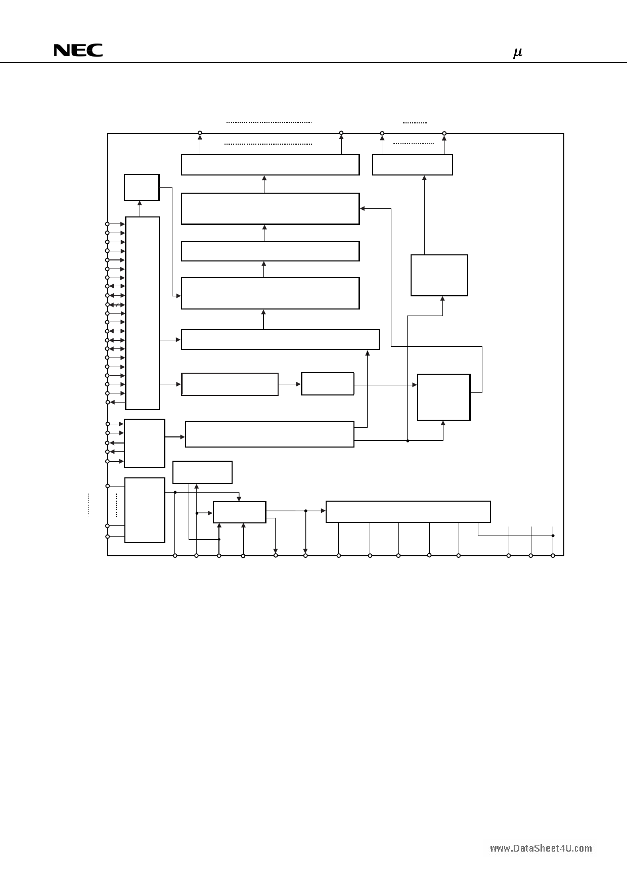
1. BLOCK DIAGRAM
SEG1
µPD16488A
SEG128
COM1
COM92
/RES
/CS1
www.DataSheet4U.comCS2
C86
PSX
/RD(E)
/WR(R,/W)
D7(SI)
D6(SCL)
D5 to D0
RS
M/S
FR
FRSYNC
DOF
SIGIN1
SIGIN2
TSTIFS
TSTRTST
TSTVIHL
TESTOUT
OSCIN1
OSCIN2
OSCOUT
OSCSYNC
CLS
C1+, C1-
C9+, C9-
C1A
Data
register
I/O
buffer
Segment driver
Segment
G/S and blink
control
Display data latch
Display data RAM
(128 x 128 x 2 bits)
Address decoder
Command decoder
Register
Oscillator
circuit
Timing generator
D/A converter
DC/DC
converter
Op amp
Common driver
Common
timing
generator
Segment
G/S and blink
timer
LCD voltage generator
VOUT VRS IRS VR AMPOUTP AMPOUT VLCD VLC1 VLC2 VLC3 VLC4
Remark /xxx indicates active low signals.
VDD1 VDD2 VSS
Data Sheet S15745EJ2V0DS
5
5 Page 
µPD16488A
Symbol
CLS
Name
Select clock
division
www.DataSheet4FUR.com
Frame signal
FRSYNC
Frame
synchronization
signal
DOF
Display blink
M/S Master/slave
IRS VLCD regulation
SIGIN1,
SIGIN2
Signature setting
pins
Pad No.
76, 77
127, 128
125, 126
130, 131
79, 80
87, 88
144, 145,
147, 148
I/O
Input
I/O
I/O
I/O
Input
(2/3)
Description
This pin is used to select whether or not to use the divider within
the display clock oscillator.
CLS = H: Use divider
CLS = L: Do not use divider
When using an external clock, the CLS = L setting is input via
the OSCIN1 and OSCIN2 pins as normal and partial clocks
respectively.
When CLS = H, clock input is via the OSCIN1 pin only.
This pin is used as I/O pin for the LCD's AC conversion signal.
M/S = H: Output
M/S = L: Input
When using the µPD16488A in master/slave mode, both FR
pins must be connected.
This pin is used as I/O pin for the LCD's AC conversion
synchronization signal.
M/S = H: Output
M/S = L: Input
When the µPD16488A is used in master/slave mode, both
FRSYNC pins must be connected.
This pin is used to control the LCD's display blink function.
M/S = H: Output
M/S = L: Input
When the µPD16488A is used in master/slave mode, both DOF
pins must be connected.
This pin is used to select between master and slave operation
modes. In master operation mode, it outputs the timing signal
required by the LCD driver and in slave operation mode it inputs
this timing signal from an external source for use in LCD display
synchronization.
M/S = H: Master operation mode
M/S = L: Slave operation mode
Settings dependent on the M/S mode are listed in the following
chart.
Power
M/S supply circuit
FR
FRSYNC
DOF
H
Valid
Output Output Output
L Invalid Input Input Input
Input
Input
This pin is used to select the resistor that is used for VLCD
voltage regulation.
IRS = H: Uses internal resistor
IRS = L: Does not use internal resistor. The VLCD voltage level
is regulated using the external voltage division resistor that is
connected to the VR pin.
This pin is valid only in master operation mode. In slave
operation mode, this pin is fixed high or low level.
These pins can be used to set a unique signature for the IC. The
signal set via these pins can subsequently be read from the
signature read register (R45).
Data Sheet S15745EJ2V0DS
11
11 Page | ||
| Páginas | Total 70 Páginas | |
| PDF Descargar | [ Datasheet D16488A.PDF ] | |
Hoja de datos destacado
| Número de pieza | Descripción | Fabricantes |
| D16488A | UPD16488A | NEC |
| Número de pieza | Descripción | Fabricantes |
| SLA6805M | High Voltage 3 phase Motor Driver IC. |
Sanken |
| SDC1742 | 12- and 14-Bit Hybrid Synchro / Resolver-to-Digital Converters. |
Analog Devices |
|
DataSheet.es es una pagina web que funciona como un repositorio de manuales o hoja de datos de muchos de los productos más populares, |
| DataSheet.es | 2020 | Privacy Policy | Contacto | Buscar |
