|
|
|
PDF AD5441 Data sheet ( Hoja de datos )
| Número de pieza | AD5441 | |
| Descripción | 12-Bit Serial Input Multiplying DAC | |
| Fabricantes | Analog Devices | |
| Logotipo | ||
Hay una vista previa y un enlace de descarga de AD5441 (archivo pdf) en la parte inferior de esta página. Total 16 Páginas | ||
|
No Preview Available !
FEATURES
2.5 V to 5.5 V supply operation
True 12-bit accuracy
5 V operation @ <1 μA
Fast 3-wire serial input
Fast 5 μs settling time
1.9 MHz, 4-quadrant multiply BW
www.DataSheeUt4pUg.craodme for DAC8043 and DAC8043A
Standard and rotated pinout
APPLICATIONS
Ideal for PLC applications in industrial control
Programmable amplifiers and attenuators
Digitally controlled calibration and filters
Motion control systems
GENERAL DESCRIPTION
The AD5441 is an improved high accuracy 12-bit multiplying
digital-to-analog converter (DAC) in space-saving 8-lead
packages. Featuring serial input, double buffering, and excellent
analog performance, the AD5441 is ideal for applications where
PC board space is at a premium. Improved linearity and gain
error performance permit reduced part counts through the
elimination of trimming components. Separate input clock and
load DAC control lines allow full user control of data loading
and analog output.
The circuit consists of a 12-bit serial-in/parallel-out shift register, a
12-bit DAC register, a 12-bit CMOS DAC, and control logic.
Serial data is clocked into the input register on the rising edge of
the clock pulse. When the new data-word is clocked in, it is
loaded into the DAC register with the LD input pin. Data in the
DAC register is converted to an output current by the DAC.
Consuming only 1 μA from a single 5 V power supply, the
AD5441 is the ideal low power, small size, high performance
solution to many application problems.
The AD5441 is specified over the extended industrial (−40°C to
+125°C) temperature range. It is available in an 8-lead LFCSP
and an 8-lead MSOP.
12-Bit Serial Input
Multiplying DAC
AD5441
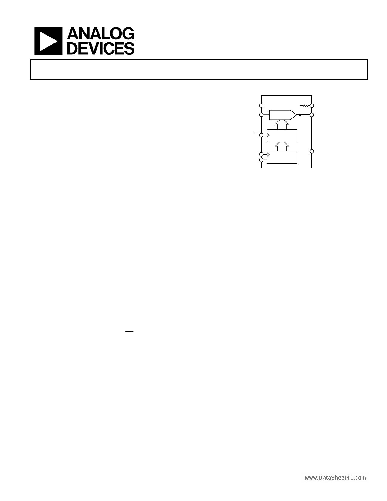
FUNCTIONAL BLOCK DIAGRAM
VDD
VREF
AD5441
DAC
RFB
IOUT
12
LD DAC REG
CLK
SRI
12
12-BIT SHIFT
REGISTER
GND
Figure 1.
Rev. 0
Information furnished by Analog Devices is believed to be accurate and reliable. However, no
responsibility is assumed by Analog Devices for its use, nor for any infringements of patents or other
rights of third parties that may result from its use. Specifications subject to change without notice. No
license is granted by implication or otherwise under any patent or patent rights of Analog Devices.
Trademarksandregisteredtrademarksarethepropertyoftheirrespectiveowners.
One Technology Way, P.O. Box 9106, Norwood, MA 02062-9106, U.S.A.
Tel: 781.329.4700
www.analog.com
Fax: 781.461.3113
©2008 Analog Devices, Inc. All rights reserved.
1 page 
ABSOLUTE MAXIMUM RATINGS
Table 4.
Parameter
VDD to GND
VREF to GND
RFB to GND
Logic Inputs to GND
IOUT to GND
IOUT Short Circuit to GND
Package Power Dissipation
Maximum Junction Temperature (TJ max)
www.DataSheeOt4pUe.rcaotming Temperature Range
Storage Temperature Range
Lead Temperature (Soldering, 10 sec)
Rating
−0.3 V, +8 V
±18 V
±18 V
−0.3 V, VDD + 0.3 V
−0.3 V, VDD + 0.3 V
50 mA
(TJ max − TA)/θJA
150°C
−40°C to +125°C
−65°C to +150°C
300°C
Stresses above those listed under Absolute Maximum Ratings
may cause permanent damage to the device. This is a stress
rating only; functional operation of the device at these or any
other conditions above those indicated in the operational
section of this specification is not implied. Exposure to absolute
maximum rating conditions for extended periods may affect
device reliability.
AD5441
THERMAL RESISTANCE
θJA is specified for the worst-case conditions, that is, a device
soldered in a circuit board for surface-mount packages.
Table 5.
Package Type
8-Lead MSOP
8-Lead LFCSP1
θJA
142
75
1 Exposed pad soldered to application board.
θJC
44
18
Unit
°C/W
°C/W
ESD CAUTION
Rev. 0 | Page 5 of 16
5 Page 
AD5441
PARAMETER DEFINITIONS
GENERAL CIRCUIT INFORMATION
The AD5441 is a 12-bit multiplying DAC with a low
temperature coefficient. It contains an R-2R resistor ladder
network, data input and control logic, and two data registers.
The digital circuitry forms an interface in which serial data can
be loaded under microprocessor control into a 12-bit shift register
and then transferred, in parallel, to the 12-bit DAC register.
The analog portion of the AD5441 contains an inverted R-2R
ladder network consisting of silicon-chrome, highly stable
www.DataShee(t540Up.cpomm/°C), thin-film resistors, and 12 pairs of NMOS current-
steering switches, see Figure 19. These switches steer binarily
weighted currents into either IOUT or GND; this yields a constant
current in each ladder leg, regardless of digital input code. This
constant current results in a constant input resistance at VREF
equal to R. The VREF input may be driven by any reference voltage
or current, ac or dc, that is within the limits stated in the
Absolute Maximum Ratings.
VREF
10kΩ
10kΩ
10kΩ
20kΩ
20kΩ
20kΩ
20kΩ
20kΩ
S1 S2 S3 S12 *
10kΩ
BIT 1 (MSB) BIT 2
BIT 3 BIT 12 (LSB)
DIGITAL INPUTS
*
*THESE SWITCHES PERMANENTLY ON.
NOTES
1. SWITCHES SHOWN FOR DIGITAL INPUTS HIGH.
Figure 19. Simplified DAC Circuit
GND
IOUT
RFEEDBACK
The 12 output current steering NMOS FET switches are in
series with each R-2R resistor.
To further ensure accuracy across the full temperature range,
MOS switches that are always on were included in series with
the feedback resistor and the terminating resistor of the R-2R
ladder. Figure 19 shows the location of the series switches.
VDD
During any testing of the resistor ladder or RFEEDBACK (such as
incoming inspection), VDD must be present to turn on these
series switches.
OUTPUT IMPEDANCE
The output resistance of the AD5441, as in the case of the
output capacitance, varies with the digital input code. This
resistance, looking back into the IOUT terminal, may be between
10 kΩ (the feedback resistor alone when all digital inputs are
low) and 7.5 kΩ (the feedback resistor in parallel with approximate
30 kΩ of the R-2R ladder network resistance when any single bit
logic is high). Static accuracy and dynamic performance are
affected by these variations.
APPLICATIONS INFORMATION
In most applications, linearity depends upon the potential of
the IOUT and GND pins being at the same voltage potential. The
DAC is connected to an external precision op amp inverting input.
The external amplifiers noninverting input should be tied directly
to ground without the usual bias current compensating resistor (see
Figure 20 and Figure 22). The selected amplifier should have a low
input bias current and low drift over temperature. The amplifiers
input offset voltage should be nulled to less than 200 mV (less than
10% of 1 LSB). All grounded pins should tie to a single common
ground point to avoid ground loops. The VDD power supply should
have a low noise level with adequate bypassing. It is best to operate
the AD5441 from the analog power supply and grounds.
UNIPOLAR 2-QUADRANT MULTIPLYING
The most straightforward application of the AD5441 is in the
2-quadrant multiplying configuration shown in Figure 20. If the
reference input signal is replaced with a fixed dc voltage reference,
the DAC output provides a proportional dc voltage output
according to the transfer equation
VOUT = −D/4096 × VREF
where:
D is the decimal data loaded into the DAC register.
VREF is the externally applied reference voltage source.
R2
VREF
R1
VDD
RFB
VREF AD5441
IOUT1
GND
LD CLK SRI
C1
A1
VOUT = 0 TO –VREF
AGND
µCONTROLLER
NOTES
1. R1 AND R2 USED ONLY IF GAIN ADJUSTMENT IS REQUIRED.
2. C1 PHASE COMPENSATION (1pF TO 2pF) MAY BE REQUIRED
IF A1 IS A HIGH SPEED AMPLIFIER.
Figure 20. Unipolar (2-Quadrant) Operation
Rev. 0 | Page 11 of 16
11 Page | ||
| Páginas | Total 16 Páginas | |
| PDF Descargar | [ Datasheet AD5441.PDF ] | |
Hoja de datos destacado
| Número de pieza | Descripción | Fabricantes |
| AD544 | High Performance/ BiFET Operational Amplifiers | Analog Devices |
| AD5440 | (AD5424 - AD5547) High Bandwidth Multiplying DACs | Analog Devices |
| AD5441 | 12-Bit Serial Input Multiplying DAC | Analog Devices |
| AD5443 | (AD5424 - AD5547) High Bandwidth Multiplying DACs | Analog Devices |
| Número de pieza | Descripción | Fabricantes |
| SLA6805M | High Voltage 3 phase Motor Driver IC. |
Sanken |
| SDC1742 | 12- and 14-Bit Hybrid Synchro / Resolver-to-Digital Converters. |
Analog Devices |
|
DataSheet.es es una pagina web que funciona como un repositorio de manuales o hoja de datos de muchos de los productos más populares, |
| DataSheet.es | 2020 | Privacy Policy | Contacto | Buscar |