|
|
|
PDF MPS651 Data sheet ( Hoja de datos )
| Número de pieza | MPS651 | |
| Descripción | (MPS650 / MPS651 / MPS750 / MPS751) Amplifier Transistors | |
| Fabricantes | ON Semiconductor | |
| Logotipo | ||
Hay una vista previa y un enlace de descarga de MPS651 (archivo pdf) en la parte inferior de esta página. Total 5 Páginas | ||
|
No Preview Available !
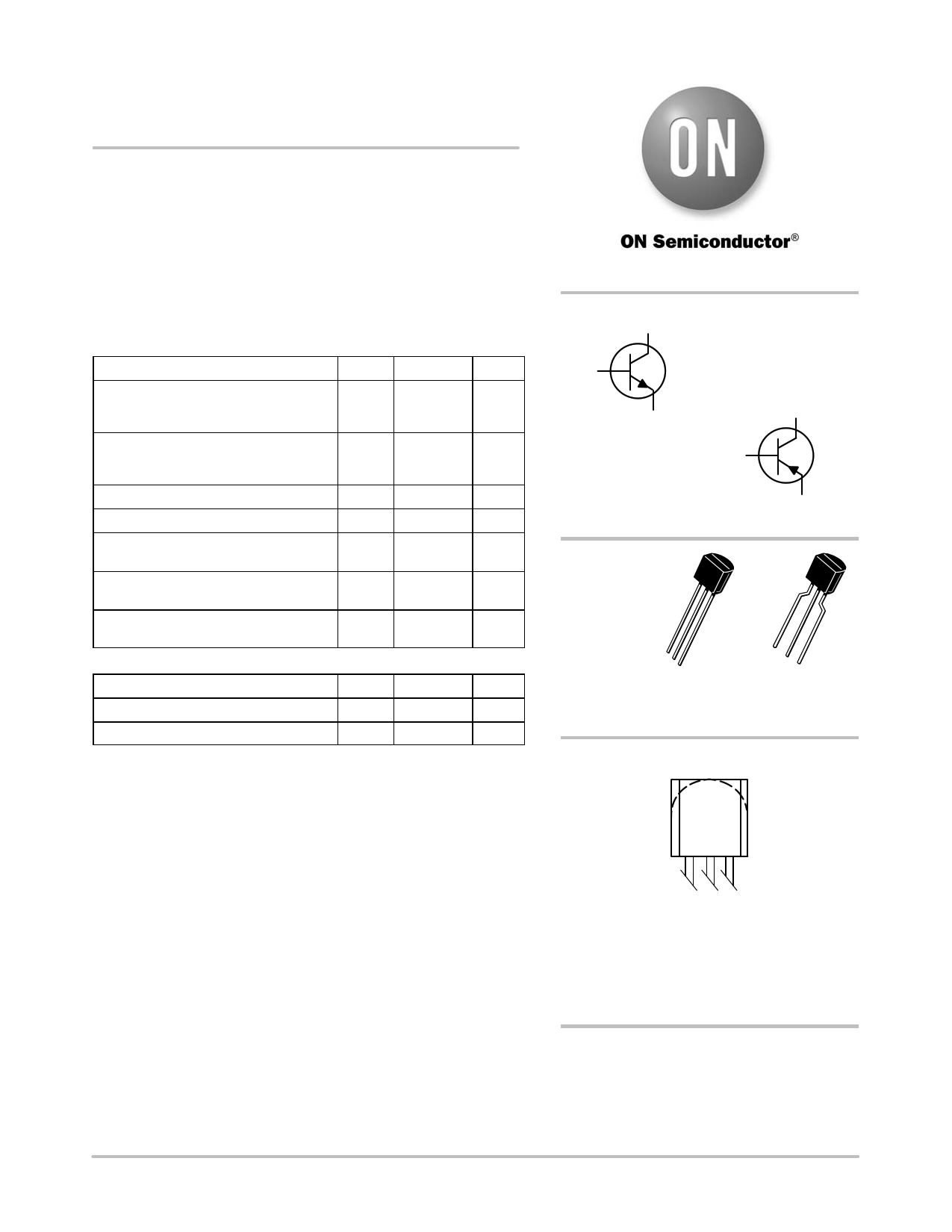
NPN - MPS650, MPS651;
PNP - MPS750, MPS751
Amplifier Transistors
Features
• These are Pb−Free Devices*
MAXIMUM RATINGS
Rating
Symbol
Collector −Emitter Voltage
MPS650; MPS750
MPS651; MPS751
VCE
Value
40
60
Unit
Vdc
Collector −Base Voltage
VCB Vdc
MPS650; MPS750
60
MPS651; MPS751
80
Emitter −Base Voltage
Collector Current − Continuous
Total Power Dissipation @ TA = 25°C
Derate above 25°C
VEB 5.0 Vdc
IC 2.0 Adc
PD 625 mW
5.0 mW/°C
Total Power Dissipation @ TC = 25°C PD 1.5 W
Derate above 25°C
12 mW/°C
Operating and Storage Junction
Temperature Range
TJ, Tstg −55 to +150 °C
THERMAL CHARACTERISTICS
Characteristic
Symbol
Max
Unit
Thermal Resistance, Junction−to−Ambient VCE
200 °C/W
Thermal Resistance, Junction−to−Case
VCB
83.3 °C/W
Stresses exceeding Maximum Ratings may damage the device. Maximum
Ratings are stress ratings only. Functional operation above the Recommended
Operating Conditions is not implied. Extended exposure to stresses above the
Recommended Operating Conditions may affect device reliability.
http://onsemi.com
COLLECTOR
3
2
BASE
NPN
1
EMITTER
COLLECTOR
3
2
BASE
PNP
1
EMITTER
TO−92
CASE 29
STYLE 1
123
STRAIGHT LEAD
BULK PACK
12 3
BENT LEAD
TAPE & REEL
AMMO PACK
MARKING DIAGRAM
AMPS
xxx
YWW G
G
xxx = 650, 750, 651, or 751
A = Assembly Location
Y = Year
WW = Work Week
G = Pb−Free Package
(Note: Microdot may be in either location)
*For additional information on our Pb−Free strategy and soldering details, please
download the ON Semiconductor Soldering and Mounting Techniques
Reference Manual, SOLDERRM/D.
© Semiconductor Components Industries, LLC, 2013
September, 2013 − Rev. 4
1
ORDERING INFORMATION
See detailed ordering and shipping information in the package
dimensions section on page 4 of this data sheet.
Publication Order Number:
MPS650/D
1 page 
NPN − MPS650, MPS651; PNP − MPS750, MPS751
PACKAGE DIMENSIONS
A
R
SEATING
PLANE
B
P
L
K
XX
H
V
G
C
1
N
N
TO−92 (TO−226)
CASE 29−11
ISSUE AM
STRAIGHT LEAD
BULK PACK
D
J
SECTION X−X
NOTES:
1. DIMENSIONING AND TOLERANCING PER ANSI
Y14.5M, 1982.
2. CONTROLLING DIMENSION: INCH.
3. CONTOUR OF PACKAGE BEYOND DIMENSION R
IS UNCONTROLLED.
4. LEAD DIMENSION IS UNCONTROLLED IN P AND
BEYOND DIMENSION K MINIMUM.
INCHES
DIM MIN MAX
A 0.175 0.205
B 0.170 0.210
C 0.125 0.165
D 0.016 0.021
G 0.045 0.055
H 0.095 0.105
J 0.015 0.020
K 0.500 ---
L 0.250 ---
N 0.080 0.105
P --- 0.100
R 0.115 ---
V 0.135 ---
MILLIMETERS
MIN MAX
4.45 5.20
4.32 5.33
3.18 4.19
0.407 0.533
1.15 1.39
2.42 2.66
0.39 0.50
12.70 ---
6.35 ---
2.04 2.66
--- 2.54
2.93 ---
3.43 ---
RAB
P
T
SEATING
PLANE
K
XX
G
V
1
C
N
BENT LEAD
TAPE & REEL
AMMO PACK
D
J
SECTION X−X
NOTES:
1. DIMENSIONING AND TOLERANCING PER
ASME Y14.5M, 1994.
2. CONTROLLING DIMENSION: MILLIMETERS.
3. CONTOUR OF PACKAGE BEYOND
DIMENSION R IS UNCONTROLLED.
4. LEAD DIMENSION IS UNCONTROLLED IN P
AND BEYOND DIMENSION K MINIMUM.
MILLIMETERS
DIM MIN MAX
A 4.45 5.20
B 4.32 5.33
C 3.18 4.19
D 0.40 0.54
G 2.40 2.80
J 0.39 0.50
K 12.70 ---
N 2.04 2.66
P 1.50 4.00
R 2.93 ---
V 3.43 ---
STYLE 1:
PIN 1.
2.
3.
EMITTER
BASE
COLLECTOR
ON Semiconductor and
are registered trademarks of Semiconductor Components Industries, LLC (SCILLC). SCILLC owns the rights to a number of patents, trademarks,
copyrights, trade secrets, and other intellectual property. A listing of SCILLC’s product/patent coverage may be accessed at www.onsemi.com/site/pdf/Patent−Marking.pdf. SCILLC
reserves the right to make changes without further notice to any products herein. SCILLC makes no warranty, representation or guarantee regarding the suitability of its products for any
particular purpose, nor does SCILLC assume any liability arising out of the application or use of any product or circuit, and specifically disclaims any and all liability, including without
limitation special, consequential or incidental damages. “Typical” parameters which may be provided in SCILLC data sheets and/or specifications can and do vary in different applications
and actual performance may vary over time. All operating parameters, including “Typicals” must be validated for each customer application by customer’s technical experts. SCILLC
does not convey any license under its patent rights nor the rights of others. SCILLC products are not designed, intended, or authorized for use as components in systems intended for
surgical implant into the body, or other applications intended to support or sustain life, or for any other application in which the failure of the SCILLC product could create a situation where
personal injury or death may occur. Should Buyer purchase or use SCILLC products for any such unintended or unauthorized application, Buyer shall indemnify and hold SCILLC and
its officers, employees, subsidiaries, affiliates, and distributors harmless against all claims, costs, damages, and expenses, and reasonable attorney fees arising out of, directly or indirectly,
any claim of personal injury or death associated with such unintended or unauthorized use, even if such claim alleges that SCILLC was negligent regarding the design or manufacture
of the part. SCILLC is an Equal Opportunity/Affirmative Action Employer. This literature is subject to all applicable copyright laws and is not for resale in any manner.
PUBLICATION ORDERING INFORMATION
LITERATURE FULFILLMENT:
Literature Distribution Center for ON Semiconductor
P.O. Box 5163, Denver, Colorado 80217 USA
Phone: 303−675−2175 or 800−344−3860 Toll Free USA/Canada
Fax: 303−675−2176 or 800−344−3867 Toll Free USA/Canada
Email: [email protected]
N. American Technical Support: 800−282−9855 Toll Free
USA/Canada
Europe, Middle East and Africa Technical Support:
Phone: 421 33 790 2910
Japan Customer Focus Center
Phone: 81−3−5817−1050
http://onsemi.com
5
ON Semiconductor Website: www.onsemi.com
Order Literature: http://www.onsemi.com/orderlit
For additional information, please contact your local
Sales Representative
MPS650/D
5 Page | ||
| Páginas | Total 5 Páginas | |
| PDF Descargar | [ Datasheet MPS651.PDF ] | |
Hoja de datos destacado
| Número de pieza | Descripción | Fabricantes |
| MPS650 | NPN SILICON PLANAR AMPLIFIER TRANSISTORS | CDIL |
| MPS650 | (MPS651) Amplifier Transistors | Motorola Semiconductors |
| MPS650 | (MPS650 / MPS651 / MPS750 / MPS751) Amplifier Transistors | ON Semiconductor |
| MPS650 | SILICON TRANSISTORS | Central Semiconductor |
| Número de pieza | Descripción | Fabricantes |
| SLA6805M | High Voltage 3 phase Motor Driver IC. |
Sanken |
| SDC1742 | 12- and 14-Bit Hybrid Synchro / Resolver-to-Digital Converters. |
Analog Devices |
|
DataSheet.es es una pagina web que funciona como un repositorio de manuales o hoja de datos de muchos de los productos más populares, |
| DataSheet.es | 2020 | Privacy Policy | Contacto | Buscar |