|
|
|
PDF LP2950 Data sheet ( Hoja de datos )
| Número de pieza | LP2950 | |
| Descripción | (LP2950 / LP2951) Low Power Low Dropout Voltage Regulator | |
| Fabricantes | ON Semiconductor | |
| Logotipo | ||
 1. PDF - Adjustable Voltage Regulator Hay una vista previa y un enlace de descarga de LP2950 (archivo pdf) en la parte inferior de esta página. Total 24 Páginas | ||
|
No Preview Available !
www.DataSheet4U.com
LP2950, LP2951, NCV2951
100 mA, Low Power Low
Dropout Voltage Regulator
The LP2950 and LP2951 are micropower voltage regulators that are
specifically designed to maintain proper regulation with an extremely
low input−to−output voltage differential. These devices feature a very
low quiescent bias current of 75 mA and are capable of supplying
output currents in excess of 100 mA. Internal current and thermal
limiting protection is provided.
The LP2951 has three additional features. The first is the Error
Output that can be used to signal external circuitry of an out of
regulation condition, or as a microprocessor power−on reset. The
second feature allows the output voltage to be preset to 5.0 V, 3.3 V or
3.0 V output (depending on the version) or programmed from 1.25 V
to 29 V. It consists of a pinned out resistor divider along with direct
access to the Error Amplifier feedback input. The third feature is a
Shutdown input that allows a logic level signal to turn−off or turn−on
the regulator output.
Due to the low input−to−output voltage differential and bias current
specifications, these devices are ideally suited for battery powered
computer, consumer, and industrial equipment where an extension of
useful battery life is desirable. The LP2950 is available in the three
pin case 29 and DPAK packages, and the LP2951 is available in the
eight pin dual−in−line, SOIC−8 and Micro8 surface mount packages.
The ‘A’ suffix devices feature an initial output voltage tolerance
± 0.5%.
Features
• Pb−Free Packages are Available
• Low Quiescent Bias Current of 75 mA
• Low Input−to−Output Voltage Differential of 50 mV at 100 mA and
380 mV at 100 mA
• 5.0 V, 3.3 V or 3.0 V ±0.5% Allows Use as a Regulator or Reference
• Extremely Tight Line and Load Regulation
• Requires Only a 1.0 mF Output Capacitor for Stability
• Internal Current and Thermal Limiting
• NCV Prefix for Automotive and Other Applications Requiring Site
and Control Changes
LP2951 Additional Features
• Error Output Signals an Out of Regulation Condition
• Output Programmable from 1.25 V to 29 V
• Logic Level Shutdown Input
(See Following Page for Device Information.)
http://onsemi.com
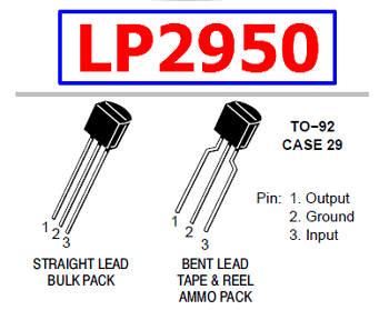
TO−92
Z SUFFIX
CASE 29
1
23
Pin: 1. Output
2. Ground
3. Input
DPAK
DT SUFFIX
CASE 369C
12
3
PIN CONNECTIONS
4
12 3
Pin: 1. Input
2. Ground
3. Output
(Top View)
Heatsink surface (shown as terminal 4 in
case outline drawing) is connected to Pin 2.
SOIC−8
D SUFFIX
CASE 751
8
1
PDIP−8
N SUFFIX
CASE 626
Micro8E
DM SUFFIX
CASE 846A
8
1
8
1
PIN CONNECTIONS
Output 1
Sense 2
Shutdown 3
GND 4
8 Input
7 Feedback
6 VO Tap
5 Error Output
(Top View)
ORDERING & MARKING INFORMATION
See detailed ordering and shipping information in the package
dimensions section on pages 14 and 16 of this data sheet.
See general marking information in the device marking
section on page 18 of this data sheet.
© Semiconductor Components Industries, LLC, 2006
December, 2006 − Rev. 19
1
Publication Order Number:
LP2950/D
1 page 
LP2950, LP2951, NCV2951
ELECTRICAL CHARACTERISTICS (continued) (Vin = VO + 1.0 V, IO = 100 mA, CO = 1.0 mF, TA = 25°C [Note 8],
unless otherwise noted.)
Characteristic
Symbol
Min
Typ
Max
Line Regulation (Vin = VO(nom) +1.0 V to 30 V) (Note 9)
LP2950C−XX/LP2951C/LP2951C−XX/NCV2951C*
LP2950AC−XX/LP2951AC/LP2951AC−XX/NCV2951AC*
Load Regulation (IO = 100 mA to 100 mA)
LP2950C−XX/LP2951C/LP2951C−XX/NCV2951C*
LP2950AC−XX/LP2951AC/LP2951AC−XX/NCV2951AC*
Dropout Voltage
IO = 100 mA
IO = 100 mA
Supply Bias Current
IO = 100 mA
IO = 100 mA
Dropout Supply Bias Current (Vin = VO(nom) − 0.5 V,
IO = 100 mA) (Note 9)
Current Limit (VO Shorted to Ground)
Regline
Regload
VI − VO
ICC
ICCdropout
ILimit
−
−
−
−
−
−
−
−
−
−
0.08 0.20
0.04 0.10
0.13 0.20
0.05 0.10
30 80
350 450
93 120
4.0 12
110 170
220 300
Thermal Regulation
Output Noise Voltage (10 Hz to 100 kHz) (Note 10)
CL = 1.0 mF
CL = 100 mF
LP2951A/LP2951AC Only
Reference Voltage (TA = 25°C)
LP2951C/LP2951C−XX/NCV2951C*
LP2951AC/LP2951AC−XX/NCV2951AC*
Reference Voltage (TA = − 40 to +125°C)
LP2951C/LP2951C−XX/NCV2951C*
LP2951AC/LP2951AC−XX/NCV2951AC*
Reference Voltage (TA = − 40 to +125°C)
IO = 100 mA to 100 mA, Vin = 23 to 30 V
LP2951C/LP2951C−XX/NCV2951C*
LP2951AC/LP2951AC−XX/NCV2951AC*
Regthermal
Vn
Vref
Vref
Vref
−
−
−
1.210
1.220
1.200
1.200
1.185
1.190
0.05
126
56
1.235
1.235
−
−
−
−
0.20
−
−
1.260
1.250
1.270
1.260
1.285
1.270
Feedback Pin Bias Current
IFB −
15 40
Error Comparator
Output Leakage Current (VOH = 30 V)
Ilkg − 0.01 1.0
Output Low Voltage (Vin = 4.5 V, IOL = 400 mA)
VOL −
150 250
Upper Threshold Voltage (Vin = 6.0 V)
Vthu
40
45
−
Lower Threshold Voltage (Vin = 6.0 V)
Vthl −
60 95
Hysteresis (Vin = 6.0 V)
Vhy − 15 −
Shutdown Input
Input Logic Voltage
Logic “0” (Regulator “On”)
Logic “1” (Regulator “Off”)
Vshtdn
0
− 0.7
2.0 − 30
Shutdown Pin Input Current
Vshtdn = 2.4 V
Vshtdn = 30 V
Ishtdn
−
−
35
450
Regulator Output Current in Shutdown Mode
Ioff − 3.0
(Vin = 30 V, Vshtdn = 2.0 V, VO = 0, Pin 6 Connected to Pin 7)
6. The Junction−to−Ambient Thermal Resistance is determined by PCB copper area per Figure 29.
7. ESD data available upon request.
8. Low duty pulse techniques are used during test to maintain junction temperature as close to ambient as possible.
9. VO(nom) is the part number voltage option.
10. Noise tests on the LP2951 are made with a 0.01 mF capacitor connected across Pins 7 and 1.
*NCV prefix is for automotive and other applications requiring site and change control.
50
600
10
Unit
%
%
mV
mA
mA
mA
mA
%/W
mVrms
V
V
V
nA
mA
mV
mV
mV
mV
V
mA
mA
http://onsemi.com
5
5 Page 
LP2950, LP2951, NCV2951
TYPICAL APPLICATIONS
+V = 2.0 to 30 V
Unregulated Input
6.0 to 10 Vdc
8
NC
5 Error
Vin
Vout
1
SNS 2 NC
0.1
mF
3
LP2951CN
SD VO T
6
NC
GND FB
47
1N4001
330 pF
2.2 mF
4.2 V ± 0.025 V
2.0 M
1.0%
806 k
1.0%
50 k
Lithium Ion
Rechargeable
Cell
GND
Figure 21. Lithium Ion Battery Cell Charger
IL Load IL = 1.23/R
Error
Output
Shutdown
Input
8
5 Error Vin Vout 1
SNS 2
LP2951CN
3 SD
VO T 6
GND FB
47
R
0.1 mF
1.0 mF
Figure 22. Low Drift Current Sink
+Vin
2N3906
470 k
8
5 Error Vin Vout 1
470 k
SNS 2 NC
Reset
LP2951CN
3 SD
VO T 6 NC
Normally
Closed
GND FB
47
R1
R2
+Vin
Vout
47 k
Error
Output
1.0 mF Shutdown
Input
*Sleep
Input
CMOS
Gate
8
5
Error
Vin
Vout
1
470 k
2N3906
Vout
SNS 2 NC
LP2951CN
3 SD
VO T 6 NC
GND FB
47
200 k
3.3 mF
100 k 100 pF
Error flag occurs when Vin is too
low to maintain Vout, or if Vout is re-
duced by excessive load current.
Figure 23. Latch Off When Error Flag Occurs
100 k
Figure 24. 5.0 V Regulator with 2.5 V Sleep Function
http://onsemi.com
11
11 Page | ||

| Páginas | Total 24 Páginas | |
| PDF Descargar | [ Datasheet LP2950.PDF ] | |
Hoja de datos destacado
| Número de pieza | Descripción | Fabricantes |
| LP2950 | 100mA LOW DROPOUT VOLTAGE REGULATOR | Advanced Monolithic Systems |
| LP2950 | 100mA Low Dropout Voltage Regulators | Calogic LLC |
| LP2950 | 100mA Low-Dropout Voltage Regulator | Micrel Semiconductor |
| LP2950 | LP295x Adjustable Micropower Voltage Regulators with Shutdown (Rev. I) | Texas Instruments |
| Número de pieza | Descripción | Fabricantes |
| SLA6805M | High Voltage 3 phase Motor Driver IC. |
Sanken |
| SDC1742 | 12- and 14-Bit Hybrid Synchro / Resolver-to-Digital Converters. |
Analog Devices |
|
DataSheet.es es una pagina web que funciona como un repositorio de manuales o hoja de datos de muchos de los productos más populares, |
| DataSheet.es | 2020 | Privacy Policy | Contacto | Buscar |