|
|
|
PDF AD5663 Data sheet ( Hoja de datos )
| Número de pieza | AD5663 | |
| Descripción | Dual 16-Bit nanoDAC | |
| Fabricantes | Analog Devices | |
| Logotipo | ||
Hay una vista previa y un enlace de descarga de AD5663 (archivo pdf) en la parte inferior de esta página. Total 24 Páginas | ||
|
No Preview Available !
www.DataSheet4U.com
2.7 V to 5.5 V, 250 μA, Rail-to-Rail Output,
Dual 16-Bit nanoDAC®
AD5663
FEATURES
Low power, dual 16-bit nanoDAC
Relative accuracy: ±12 LSBs maximum
Guaranteed monotonic by design
10-lead MSOP and 3 mm × 3 mm LFCSP_WD
2.7 V to 5.5 V power supply
Per channel power-down
Power-on reset to zero scale or midscale
Hardware LDAC and CLR functions
Serial interface; up to 50 MHz
APPLICATIONS
Process control
Data acquisition systems
Portable battery-powered instruments
Digital gain and offset adjustment
Programmable voltage and current sources
Programmable attenuators
GENERAL DESCRIPTION
The AD5663, a member of the nanoDAC family, is a low power,
dual, 16-bit buffered voltage-out DAC that operates from a single
2.7 V to 5.5 V supply and is guaranteed monotonic by design.
The AD5663 requires an external reference voltage to set the
output range of the DAC. The part incorporates a power-on
reset circuit that ensures the DAC output powers up to 0 V or
midscale (AD5663-1) and remains there until a valid write takes
place. The part contains a power-down feature that reduces the
current consumption of the device to 480 nA at 5 V and provides
software-selectable output loads while in power-down mode.
The low power consumption of this part in normal operation
makes it ideally suited to portable, battery-operated equipment.
The power consumption is 1.25 mW at 5 V, going down to
2.4 μW in power-down mode.
The on-chip precision output amplifier of the AD5663 allows
rail-to-rail output swing to be achieved.
The AD5663 uses a versatile, 3-wire serial interface that
operates at clock rates up to 50 MHz and is compatible with
standard SPI®, QSPI™, MICROWIRE™, and DSP interface
standards.
SCLK
SYNC
DIN
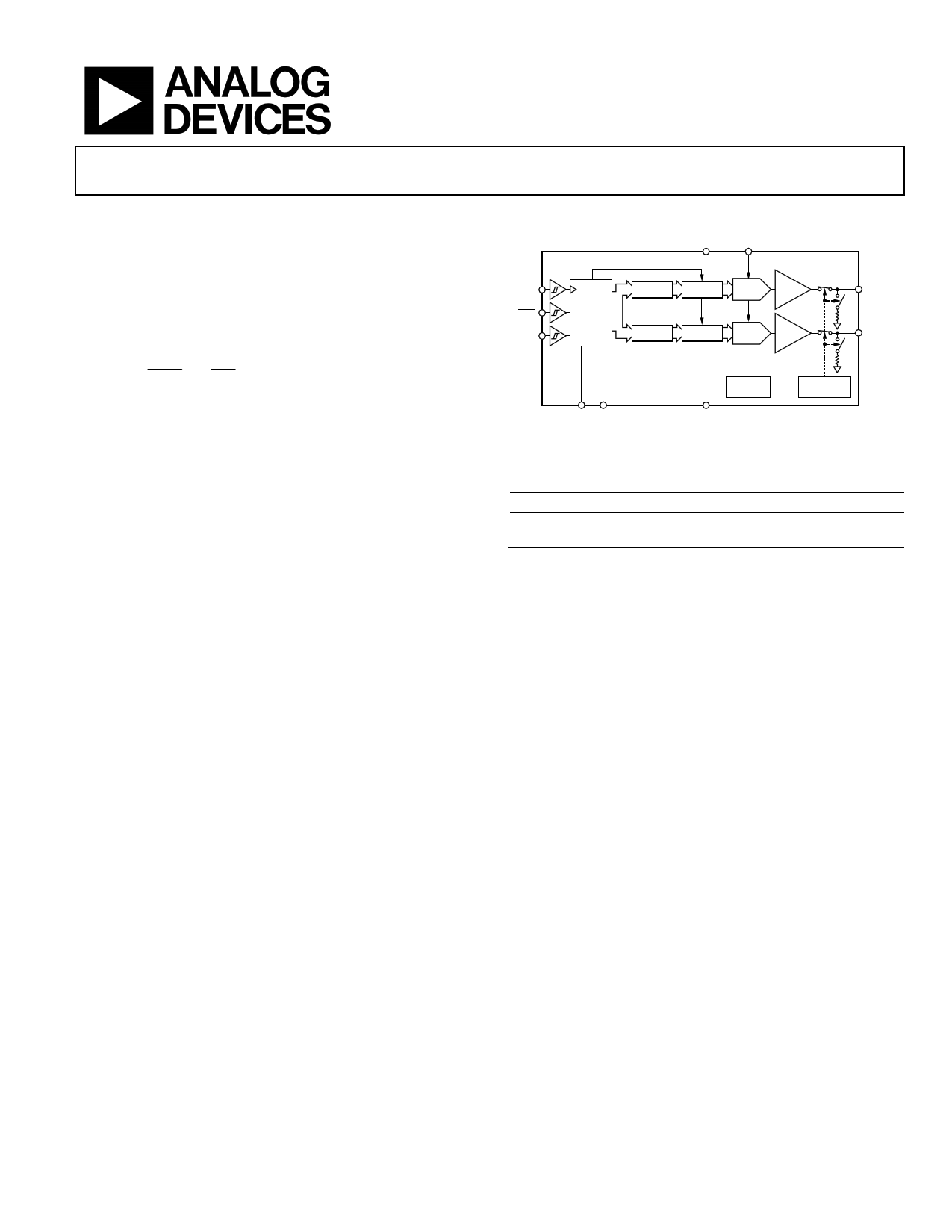
FUNCTIONAL BLOCK DIAGRAM
VDD
VREF
LDAC
INTERFACE
LOGIC
INPUT
REGISTER
DAC
REGISTER
STRING
DAC A
BUFFER
INPUT
REGISTER
DAC
REGISTER
STRING
DAC B
BUFFER
VOUTA
VOUTB
LDAC CLR
AD5663
POWER-ON
RESET
GND
Figure 1.
POWER-DOWN
LOGIC
Table 1. Related Devices
Part No.
AD5623R/AD5643R/AD5663R
Description
2.7 V to 5.5 V, dual 12-/14-/16-bit
DACs with internal reference
PRODUCT HIGHLIGHTS
1. Dual 16-bit DAC; relative accuracy of ±12 LSBs maximum.
2. Available in 10-lead MSOP and 10-lead, 3 mm × 3 mm
LFCSP_WD packages.
3. Low power; typically consumes 0.6 mW at 3 V and
1.25 mW at 5 V.
4. 7 μs maximum settling time.
Rev. 0
Information furnished by Analog Devices is believed to be accurate and reliable. However, no
responsibility is assumed by Analog Devices for its use, nor for any infringements of patents or other
rights of third parties that may result from its use. Specifications subject to change without notice. No
license is granted by implication or otherwise under any patent or patent rights of Analog Devices.
Trademarksandregisteredtrademarksarethepropertyoftheirrespectiveowners.
One Technology Way, P.O. Box 9106, Norwood, MA 02062-9106, U.S.A.
Tel: 781.329.4700
www.analog.com
Fax: 781.461.3113
©2006 Analog Devices, Inc. All rights reserved.
1 page 
TIMING CHARACTERISTICS
All input signals are specified with tR = tF = 1 ns/V (10% to 90% of VDD) and timed from a voltage level of (VIL + VIH)/2.
VDD = 2.7 V to 5.5 V; all specifications TMIN to TMAX, unless otherwise noted.1
Table 4.
Parameter
t1 2
t2
t3
t4
t5
t6
t7
t8
t9
t10
t11
t12
t13
t14
t15
Limit at TMIN, TMAX
VDD = 2.7 V to 5.5 V
20
9
9
13
5
5
0
15
13
0
10
15
5
0
300
Unit
ns min
ns min
ns min
ns min
ns min
ns min
ns min
ns min
ns min
ns min
ns min
ns min
ns min
ns min
ns max
Conditions/Comments
SCLK cycle time
SCLK high time
SCLK low time
SYNC to SCLK falling edge setup time
Data setup time
Data hold time
SCLK falling edge to SYNC rising edge
Minimum SYNC high time
SYNC rising edge to SCLK fall ignore
SCLK falling edge to SYNC fall ignore
LDAC pulse width low
SCLK falling edge to LDAC rising edge
CLR pulse width low
SCLK falling edge to LDAC falling edge
CLR pulse activation time
1 Guaranteed by design and characterization; not production tested.
2 Maximum SCLK frequency is 50 MHz at VDD = 2.7 V to 5.5 V.
TIMING DIAGRAM
SCLK
SYNC
DIN
LDAC1
t10
t8 t4
DB23
t6
t5
LDAC2
CLR
t13
VOUT
t15
1ASYNCHRONOUS LDAC UPDATE MODE.
2SYNCHRONOUS LDAC UPDATE MODE.
t1
t3 t2
t9
t7
DB0
t14
t11
t12
Figure 2. Serial Write Operation
AD5663
Rev. 0 | Page 5 of 24
5 Page 
16
VREF = VDD
TA = 25°C
14
12
VDD = 3V
10
8 VDD = 5V
6
4
0 1 2 3 4 5 6 7 8 9 10
CAPACITANCE (nF)
Figure 22. Settling Time vs. Capacitive Load
VDD = VREF = 5V
TA = 25°C
DAC LOADED WITH MIDSCALE
1
Y AXIS = 2µV/DIV
X AXIS = 4s/DIV
Figure 23. 0.1 Hz to 10 Hz Output Noise Plot
800
VDD = VREF = 5V
700 TA = 25°C
600
500
400
300
200
100
0
10
100 1k 10k 100k
FREQUENCY (Hz)
Figure 24. Noise Spectral Density
1M
AD5663
5
0
–5
–10
–15
–20
–25
–30
–35
–40
10k
VDD = 5V
TA = 25°C
100k
1M
FREQUENCY (Hz)
Figure 25. Multiplying Bandwidth
10M
3
VOUT A
CLR
VOUT B
4
2
CH3 5.0V
CH2 1.0V
CH4 1.0V
M200ns A CH3
Figure 26. CLR Pulse Activation Time
1.10V
Rev. 0 | Page 11 of 24
11 Page | ||
| Páginas | Total 24 Páginas | |
| PDF Descargar | [ Datasheet AD5663.PDF ] | |
Hoja de datos destacado
| Número de pieza | Descripción | Fabricantes |
| AD5660 | 12-/14-/16-Bit nanoDAC | Analog Devices |
| AD5662 | 2.7 V to 5.5 V 250 uA Rail-to-Rail Output 16-Bit DAC D/A | Analog Devices |
| AD5663 | Dual 16-Bit nanoDAC | Analog Devices |
| AD5663R | (AD5623R - AD5663R) nanoDAC | Analog Devices |
| Número de pieza | Descripción | Fabricantes |
| SLA6805M | High Voltage 3 phase Motor Driver IC. |
Sanken |
| SDC1742 | 12- and 14-Bit Hybrid Synchro / Resolver-to-Digital Converters. |
Analog Devices |
|
DataSheet.es es una pagina web que funciona como un repositorio de manuales o hoja de datos de muchos de los productos más populares, |
| DataSheet.es | 2020 | Privacy Policy | Contacto | Buscar |