|
|
|
PDF ADG2108 Data sheet ( Hoja de datos )
| Número de pieza | ADG2108 | |
| Descripción | I2C CMOS 8 x 10 Unbuffered Analog Switch Array | |
| Fabricantes | Analog Devices | |
| Logotipo | ||
Hay una vista previa y un enlace de descarga de ADG2108 (archivo pdf) en la parte inferior de esta página. Total 28 Páginas | ||
|
No Preview Available !
www.DataSheet4U.com
I2C® CMOS 8 × 10 Unbuffered Analog
Switch Array with Dual/Single Supplies
ADG2108
FEATURES
I2C-compatible interface
3.4 MHz high speed I2C option
32-lead LFCSP_VQ (5 mm × 5 mm)
Double-buffered input logic
Simultaneous update of multiple switches
Up to 300 MHz bandwidth
Fully specified at dual ±5 V/single +12 V operation
On resistance 35 Ω maximum
Low quiescent current < 20 μA
APPLICATIONS
AV switching in TV
Automotive infotainment
AV receivers
CCTV
Ultrasound applications
KVM switching
Telecom applications
Test equipment/instrumentation
PBX systems
GENERAL DESCRIPTION
The ADG2108 is an analog cross point switch with an
array size of 8 × 10. The switch array is arranged so that
there are eight columns by 10 rows, for a total of 80 switch
channels. The array is bidirectional, and the rows and columns
can be configured as either inputs or outputs. Each of the 80
switches can be addressed and configured through the I2C-
compatible interface. Standard, full speed, and high speed
(3.4 MHz) I2C interfaces are supported. Any simultaneous
switch combination is allowed. An additional feature of the
ADG2108 is that switches can be updated simultaneously,
using the LDSW command. In addition, a RESET option
allows all of the switch channels to be reset/off. At power on,
all switches are in the off condition. The device is packaged
in a 32-lead, 5 mm × 5 mm LFCSP_VQ.
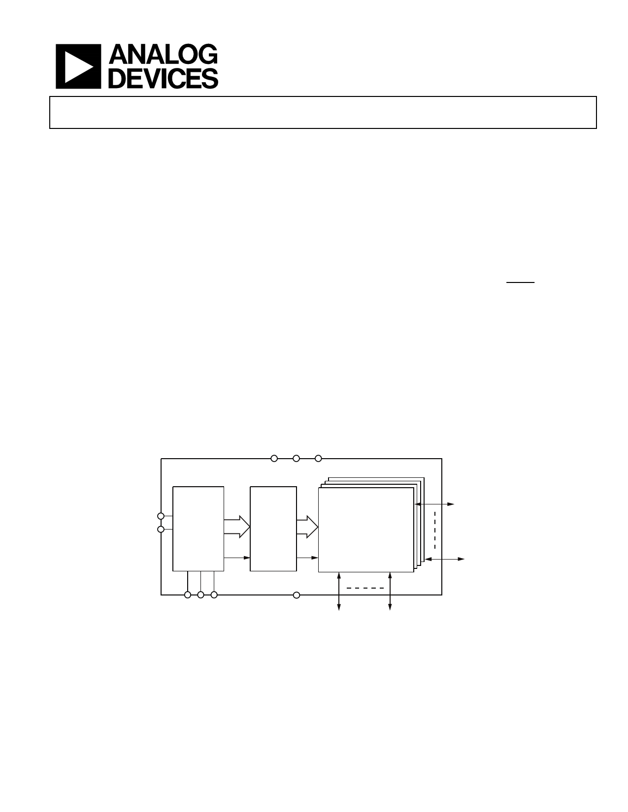
ADG2108
FUNCTIONAL BLOCK DIAGRAM
VDD VSS
VL
SCL
SDA
INPUT
REGISTER
AND
7 TO 80
DECODER
1
80
1
LATCHES
80
LDSW
LDSW
8 × 10 SWITCH ARRAY
X0 TO X9 (I/O)
A2 A1 A0
GND
Y0 TO Y7 (I/O)
Figure 1.
Rev. 0
Information furnished by Analog Devices is believed to be accurate and reliable. However, no
responsibility is assumed by Analog Devices for its use, nor for any infringements of patents or other
rights of third parties that may result from its use. Specifications subject to change without notice. No
license is granted by implication or otherwise under any patent or patent rights of Analog Devices.
Trademarksandregisteredtrademarksarethepropertyoftheirrespectiveowners.
One Technology Way, P.O. Box 9106, Norwood, MA 02062-9106, U.S.A.
Tel: 781.329.4700
www.analog.com
Fax: 781.461.3113
©2006 Analog Devices, Inc. All rights reserved.
1 page 
ADG2108
VDD = +5 V ± 10%, VSS = −5 V ± 10%, VL = 5 V, GND = 0 V, all specifications TMIN to TMAX, unless otherwise noted.1
Table 2.
Parameter
ANALOG SWITCH
Analog Signal Range
On Resistance, RON
On Resistance Matching
Between Channels, ∆RON
On Resistance Flatness, RFLAT(ON)
LEAKAGE CURRENTS
Channel Off Leakage, IOFF
Channel On Leakage, ION
DYNAMIC CHARACTERISTICS2
COFF
CON
tON
tOFF
THD + N
PSRR
−3 dB Bandwidth
Off Isolation
Channel-to-Channel Crosstalk
Adjacent Channels
Nonadjacent Channels
Differential Gain
Differential Phase
Charge Injection
LOGIC INPUTS (Ax, RESET)2
B Version
−40°C to
+25°C +125°C
34
40 45
50
55 65
66
75 85
4.5
89
17
20 23
34
42 45
±0.03
±0.03
6
9.5
170
200 215
210
250 255
0.04
300
18
−66
−62
−79
1.5
1.8
−3
Y Version
−40°C to
+25°C +125°C
VDD − 2 V
34
40 50
50
55 70
66
75 95
4.5
8 10
17
20 25
34
42 48
±0.03
±0.03
6
9.5
170
200 220
210
250 260
0.04
90
300
18
−64
−62
−79
1.5
1.8
−3
Unit
V max
Ω typ
Ω max
Ω typ
Ω max
Ω typ
Ω max
Ω typ
Ω max
Ω typ
Ω max
Ω typ
Ω max
μA typ
μA typ
pF typ
pF typ
ns typ
ns max
ns typ
ns max
% typ
dB typ
MHz typ
MHz typ
dB typ
dB typ
dB typ
% typ
° typ
pC typ
Conditions
VDD = +4.5 V, VSS = −4.5 V, VIN = VSS, IS = −10 mA
VDD = +4.5 V, VSS = −4.5 V, VIN = 0 V, IS = −10 mA
VDD = +4.5 V, VSS = −4.5 V, VIN = 1.4 V, IS = −10 mA
VDD = +4.5 V, VSS = −4.5 V, VIN = VSS, IS = −10 mA
VDD = +4.5 V, VSS = −4.5 V, VIN = VSS to 0 V, IS = −10 mA
VDD = +4.5 V, VSS = −4.5 V, VIN = VSS to 1.4 V, IS = −10 mA
VDD = 5.5 V, VSS = 5.5 V
VX = +4.5 V/−2 V, VY = −2 V/+4.5 V
VX = VY = −2 V or +4.5 V
RL = 300 Ω, CL = 35 pF
RL = 300 Ω, CL = 35 pF
RL = 10 kΩ, f = 20 Hz to 20 kHz, VS = 1 V p-p
f = 20 kHz; without decoupling; see Figure 24
Individual inputs to outputs
8 inputs to 1 output
RL = 75 Ω, CL = 5 pF, f = 5 MHz
RL = 75 Ω, CL = 5 pF, f = 5 MHz
RL = 75 Ω, CL = 5 pF, f = 5 MHz
RL = 75 Ω, CL = 5 pF, f = 5 MHz
VS = 0 V, RS = 0 Ω, CL = 1 nF
Input High Voltage, VINH
Input Low Voltage, VINL
Input Leakage Current, IIN
Input Capacitance, CIN
LOGIC INPUTS (SCL, SDA)2
Input High Voltage, VINH
Input Low Voltage, VINL
0.005
7
2.0
0.8
±1
0.005
7
2.0
0.8
±1
V min
V max
μA typ
μA max
pF typ
0.7 VL
VL + 0.3
−0.3
0.3 VL
0.7 VL
VL + 0.3
−0.3
0.3 VL
V min
V max
V min
V max
Rev. 0 | Page 5 of 28
5 Page 
TYPICAL PERFORMANCE CHARACTERISTICS
200
180
TIDAS
= 25°C
= 10mA
160
140 VDVDSS==+80VV
120
VVDSDS
=
=
–5V
+5V
100
80
60
40
VDVDS=S
= 0V
+12V
20
0
–5 –4 –3 –2 –1 0 1 2 3 4 5 6 7 8 9 10 11 12
SOURCE VOLTAGE (V)
Figure 4. Signal Range
85
TA = 25°C
IDS = 10mA
75
65
55
VDD/VSS = ±4.5V
VDD/VSS = ±5V
45
VDD/VSS = ±5.5V
35
25
–5.5 –4.5 –3.5 –2.5 –1.5 –0.5
SOURCE VOLTAGE (V)
0.5
1.5
Figure 5. RON vs. Source Voltage, Dual ±5 V Supplies
70
TA = 25°C
65 IDS = 10mA
60
VDD = 10.8V
55
50 VDD = 12V
45
40
35
VDD = 13.2V
30
25
20
01234567
SOURCE VOLTAGE (V)
8
Figure 6. RON vs. Supplies, VDD = 12 V ± 10%
ADG2108
90
TA = 25°C
IDS = 10mA
80
70
60
VDD = 7.2V
VDD = 8V
50
VDD = 8.8V
40
30
0 0.5 1.0 1.5 2.0 2.5 3.0 3.5 4.0 4.5 5.0
SOURCE VOLTAGE (V)
Figure 7. RON vs. Source Voltage, VDD = 8 V ± 10%
80
VDD = +5V
70
VSS = –5V
IDS = 10mA
60
50
TA = +125°C
TA = +85°C
40
TA = +25°C
30
TA = –40°C
20
10
0
–5 –4 –3 –2 –1
0
SOURCE VOLTAGE (V)
1
Figure 8. RON vs. Temperature, Dual ±5 V Supplies
60
VDD = 12V
VSS = 0V
50 IDS = 10mA
TA = +125°C
TA = +85°C
40
30 TA = +25°C
TA = –40°C
20
10
0
012345
SOURCE VOLTAGE (V)
Figure 9. RON vs. Temperature, VDD = 12 V
6
Rev. 0 | Page 11 of 28
11 Page | ||
| Páginas | Total 28 Páginas | |
| PDF Descargar | [ Datasheet ADG2108.PDF ] | |
Hoja de datos destacado
| Número de pieza | Descripción | Fabricantes |
| ADG2108 | I2C CMOS 8 x 10 Unbuffered Analog Switch Array | Analog Devices |
| Número de pieza | Descripción | Fabricantes |
| SLA6805M | High Voltage 3 phase Motor Driver IC. |
Sanken |
| SDC1742 | 12- and 14-Bit Hybrid Synchro / Resolver-to-Digital Converters. |
Analog Devices |
|
DataSheet.es es una pagina web que funciona como un repositorio de manuales o hoja de datos de muchos de los productos más populares, |
| DataSheet.es | 2020 | Privacy Policy | Contacto | Buscar |