|
|
PDF LM3207 Data sheet ( Hoja de datos )
| Número de pieza | LM3207 | |
| Descripción | Step-Down DC-DC Converter | |
| Fabricantes | National Semiconductor | |
| Logotipo | ||
Hay una vista previa y un enlace de descarga de LM3207 (archivo pdf) en la parte inferior de esta página. Total 24 Páginas | ||
|
No Preview Available !
April 2007
LM3207
650mA Miniature, Adjustable, Step-Down DC-DC Converter
for RF Power Amplifiers with Integrated Vref LDO
General Description
The LM3207 is a DC-DC converter optimized for powering
WCDMA / CDMA RF power amplifiers (PAs) from a single
Lithium-Ion cell; however they may be used in many other
applications. It steps down an input voltage from 2.7V to 5.5V
to a variable output voltage from 0.8V(typ.) to 3.6V(typ.). Out-
put voltage is set using a VCON analog input for controlling
power levels and efficiency of the RF PA.
The LM3207 also provides a regulated reference voltage
(Vref) required by linear RF power amplifiers through an in-
tegrated LDO that has a maximum Iref up to 10 mA. See
Ordering Information table on page 2 for Voltage Options.
The LM3207 is available in a 9-pin lead free micro SMD pack-
age. High switching frequency (2MHz) allows use of surface-
mount components. Only four small external surface-mount
components are required, an inductor and three ceramic ca-
pacitors.
Features
■ 2MHz (typ.) PWM Switching Frequency
■ Operates from a single Li-Ion cell (2.7V to 5.5V)
■ Variable Output Voltage (0.8V to 3.6V)
■ 650mA Maximum load capability
■ High Efficiency (95% Typ at 3.9VIN, 3.4VOUT at 400mA)
from internal synchronous rectification
■ Integrated Vref LDO
■ Regulated LDO Output up to 10mA max
■ Fast 3uS Vref LDO On/Off Time
■ 9-pin micro SMD Package
■ Current Overload Protection
■ Thermal Overload Protection
Applications
■ Cellular Phones
■ Hand-Held Radios
■ RF PC Cards
■ Battery Powered RF Devices
Typical Application
FIGURE 1. LM3207 Typical Application
20165301
© 2007 National Semiconductor Corporation 201653
www.national.com
1 page 
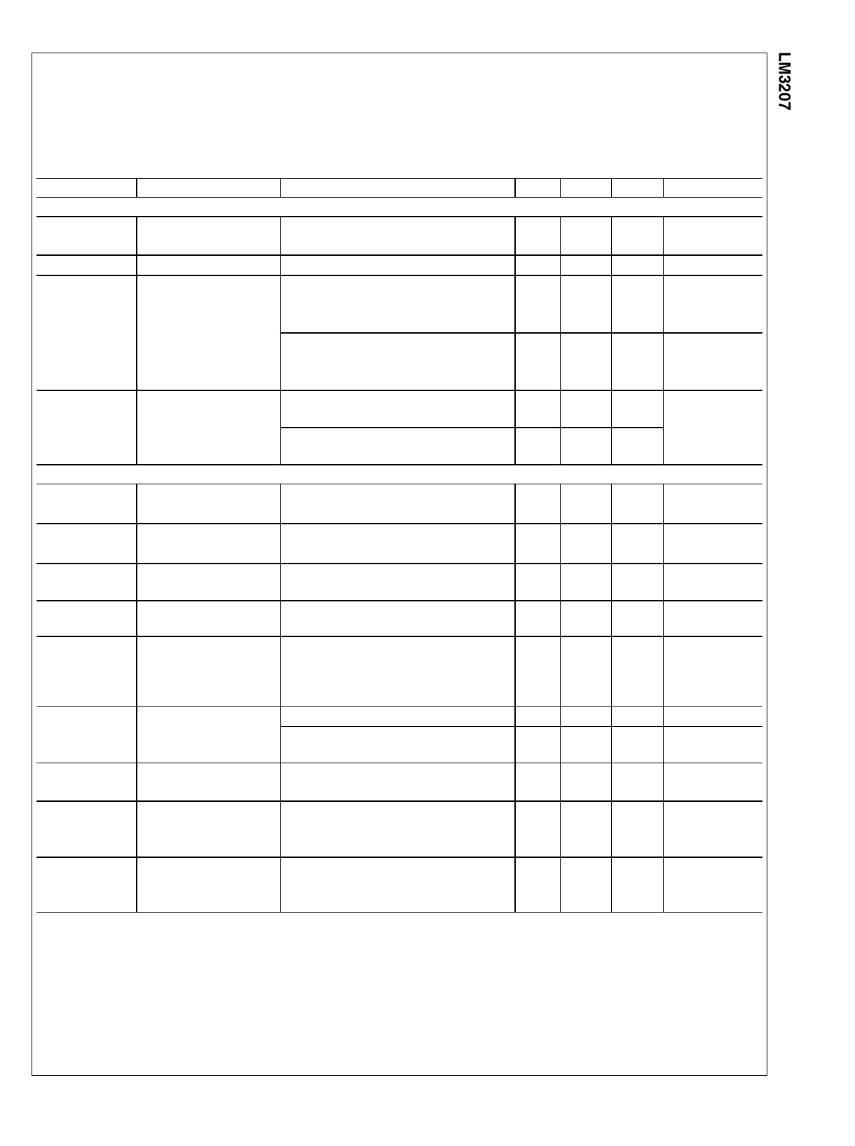
System Characteristics The following spec table entries are guaranteed by design providing the component
values in the typical application circuit are used (L = 3.0µH, (DCR = 0.12Ω, FDK MIPW3226D3R0M);
CIN = 10µF, (6.3V, 0805, TDK C2012X5R0J106K); COUT = 4.7µF, (6.3V, 0603, TDK C1608X5R0J475M); CLDO = 100nF, (10V,
0402, TDK C1005X5R1A104KT) (or 220nF, (6.3V, 0402, TDK C1005X5R0J224KT))) . These parameters are not guaranteed
by production testing. Min and Max values are specified over the VIN range = 2.7V to 5.5V and over the ambient temp range
TA = −30°C to 85°C unless otherwise specified. Typical values are specified at PVIN = EN = 3.6V and TA = 25°C unless otherwise
specified.
Symbol
Parameter
Conditions
Min
LDO
PSRR
VLDO(NOISE)
tLDO, ON
tLDO, OFF
Power Supply Rejection
Ratio
Output Noise Voltage
Time to reach 90% of
VLDO(nom) after ENLDO
signal goes high.
Time to reach 10% of
VLDO(nom) after ENLDO
signal goes low.
Offset Freq = 1Khz, Cout = 100nF,
Iout = 1mA, PVin = Vout(nom) + 0.5V
BW = 10Hz to 100Khz, Iout = 1mA
CLDO = 100nF, PWM mode assumed to be
fully functional before ENLDO goes high.
PVin = 3V, RLOAD = 562 Ω (Note 12)
CLDO = 220nF, PWM mode assumed to be
fully functional before ENLDO goes high.
PVin = 3V, RLOAD = 562 Ω (Note 12)
CLDO = 100nF, PVin = 3V, Iout = 0mA
(Note 12)
CLDO = 220nF, PVin = 3V, Iout = 0mA
(Note 12)
Switcher
TRESPONSE (Rise
time)
TRESPONSE (Fall
time)
CCON
Time for VOUT to rise from PVIN = 4.2V, COUT = 4.7uF, L = 3.0uH,
0.8V to 3.6V
RLOAD = 5.5Ω
Time for VOUT to fall from PVIN = 4.2V, COUT = 4.7uF, L = 3.0uH,
3.6V to 0.8V
RLOAD = 10Ω
VCON input capacitance VCON = 1V,
Test frequency = 100 kHz
VCON Linearity
Linearity in control
range 0.32V to 1.44V
PVIN = 3.9V, Monotonic in nature
-3
T_ON
Turn on time
(time for output to reach
3.6V from Enable low to
high transition)
EN = Low to High, PVIN = 4.2V,
VO = 3.6V, COUT = 4.7µF,
IOUT ≤ 1mA
η Efficiency PVIN = 3.6V, VOUT = 0.8V, IOUT = 90mA
(L = 3.0µH, DCR ≤
PVIN = 3.9V, VOUT = 3.4V, IOUT = 400mA
100mΩ)
VO_ripple
Line_tr
Load_tr
Ripple voltage, PWM
mode
Line transient response
Load transient response
PVIN = 3V to 4.5V, VOUT = 0.8V,
IOUT = 10mA to 400mA, (Note 11)
PVIN = 600mV perturbance,
TRISE = TFALL = 10µs, VOUT = 0.8V,
IOUT = 100mA
PVIN = 3.1/3.6/4.5V, VOUT = 0.8V,
transients up to 100mA,
TRISE = TFALL = 10µs
Typ
50
30
20
20
70
81
95
10
50
50
Max Units
dB
uVrms
3 uS
5 uS
3
uS
5
30 µs
30 µs
20 pF
+3 %
100 µs
%
%
mVp-p
mV
mV
Note 1: Absolute Maximum Ratings indicate limits beyond which damage to the component may occur. Operating Ratings are conditions under which operation
of the device is guaranteed. Operating Ratings do not imply guaranteed performance limits. For guaranteed performance limits and associated test conditions,
see the Electrical Characteristics tables.
Note 2: All voltages are with respect to the potential at the GND pins. The LM3207 is designed for mobile phone applications where turn-on after power-up is
controlled by the system controller and where requirements for a small package size overrule increased die size for internal Under Voltage Lock-Out (UVLO)
circuitry. Thus, it should be kept in shutdown by holding the EN pin low until the input voltage exceeds 2.7V.
Note 3: Internal thermal shutdown circuitry protects the device from permanent damage. Thermal shutdown engages at TJ = 150°C (typ.) and disengages at TJ
= 130°C (typ.).
5 www.national.com
5 Page 
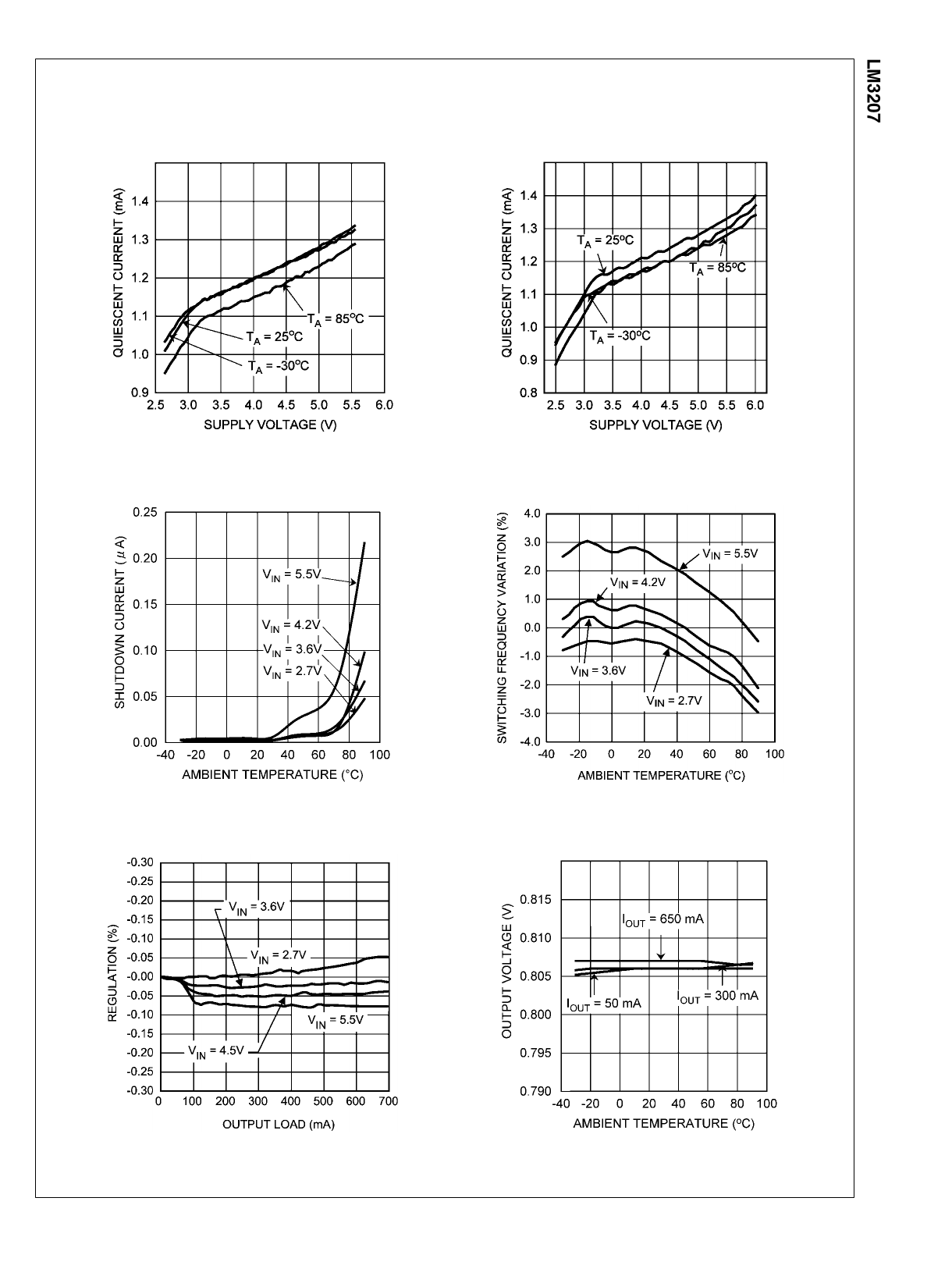
SWITCHER Typical Performance Curves
Quiescent Current vs Supply Voltage
(VCON = 2V, FB = 0V, No Switching, LDO Disabled)
Quiescent Current vs Supply Voltage
(VCON = 2V, FB = 0V, No Switching, LDO Enabled)
20165315
Shutdown Current vs Temperature
(VCON = 0V, EN = 0V)
20165379
Switching Frequency vs Temperature
(VOUT = 1.3V, IOUT = 200mA)
20165303
Output Voltage Regulation(%) vs Output Load
(VOUT = 1.5V)
20165302
Output Voltage vs Temperature
(VIN = 3.6V, VOUT = 0.8V)
20165316
11
20165317
www.national.com
11 Page | ||
| Páginas | Total 24 Páginas | |
| PDF Descargar | [ Datasheet LM3207.PDF ] | |
Hoja de datos destacado
| Número de pieza | Descripción | Fabricantes |
| LM320 | Series 3-Terminal Negative Regulators | National Semiconductor |
| LM320 | LM120/LM320 Series 3-Terminal Negative Regulators (Rev. C) | Texas Instruments |
| LM3200 | LM3200 Mini Adj Step-Down DC-DC Cnvrt w/Bypass Mode for RF Pwr Amp (Rev. C) | Texas Instruments |
| LM3200 | Step-Down DC-DC Converter with Bypass Mode for RF Power Amplifiers | National Semiconductor |
| Número de pieza | Descripción | Fabricantes |
| SLA6805M | High Voltage 3 phase Motor Driver IC. |
Sanken |
| SDC1742 | 12- and 14-Bit Hybrid Synchro / Resolver-to-Digital Converters. |
Analog Devices |
|
DataSheet.es es una pagina web que funciona como un repositorio de manuales o hoja de datos de muchos de los productos más populares, |
| DataSheet.es | 2020 | Privacy Policy | Contacto | Buscar |
