|
|
PDF STV9390 Data sheet ( Hoja de datos )
| Número de pieza | STV9390 | |
| Descripción | Class-D Vertical Defleection Amplifier | |
| Fabricantes | ST Microelectronics | |
| Logotipo |  |
|
Hay una vista previa y un enlace de descarga de STV9390 (archivo pdf) en la parte inferior de esta página. Total 7 Páginas | ||
|
No Preview Available !
STV9390
CLASS-D VERTICAL DEFLECTION AMPLIFIER FOR TV AND
MONITOR APPLICATION
FEATURES
s HIGH EFFICIENCY POWER AMPLIFIER
s NO HEATSINK
s SPLIT SUPPLY
ms INTERNAL FLYBACK GENERATOR
s OUTPUT CURRENT UP TO 2.2 APP
os SUITABLE FOR DC COUPLING
.cAPPLICATION
s FEW EXTERNAL COMPONENTS
t4Us PROTECTION AGAINST LOW Vcc
SO20
ORDER CODE: STV9390
heeDESCRIPTION
SDesigned for monitors and TVs, the STV9390 is a
class-D vertical deflection booster assembled in
taSO20 Package.
It operates with supplies up to +/- 18V, provides
up to 2.2 App output current to drive the yoke. The
ainternal flyback generator avoids the need for an
www.Dextra power supply.
PIN CONNECTION
+VCC
+VCC POW
-VCC POW
NC
-VCC
-VCC
NC
OUT
CFLY+
CFLY-
1
2
3
4
5
6
7
8
9
10
20 EAOUT
19 IN+
18 IN-
17 SGND
16 -VCC
15 -VCC
14 FREQ
13 FEEDCAP
12 VREG
11 BOOT
September 2003
www.DataSheVeerstio4nU21./170.com
1 page 
STV9390
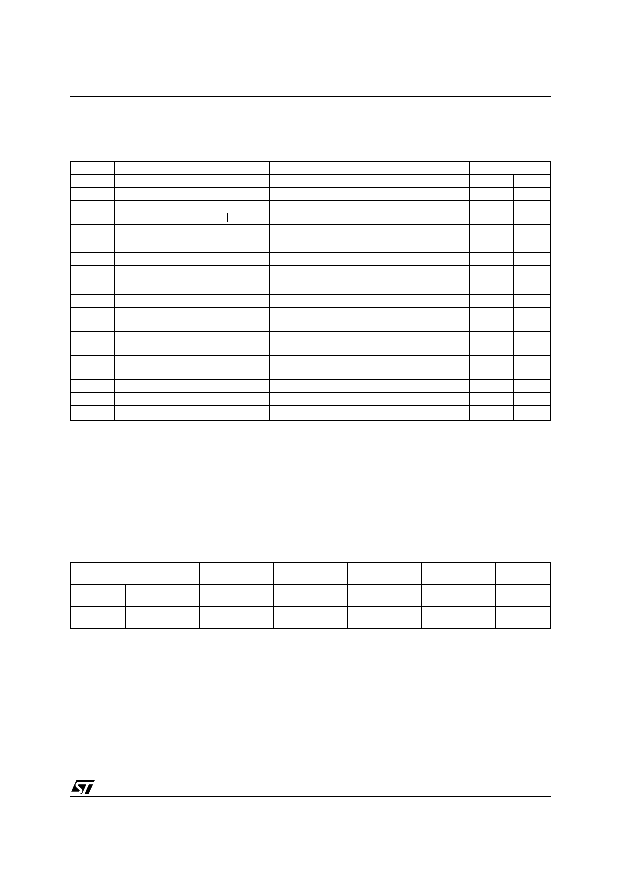
5 ELECTRICAL CHARACTERISTICS (refer to Figure 1 on page 3)
Tamb = 25°C unless otherwise specified, Vcc = ±12V, fvert=50Hz
Symbol
+Vcc
-Vcc
∆Vcc
Vccstart
Iq
Iy
I13, I12
VOS
SVR
Flythr
Flythf
Pd
Fsw
Fsw - op
Rfreq
Parameter
Test Conditions
Positive supply range
Negative supply range
Maximum recommended difference
between +Vcc and –Vcc
Low Vcc detection
Quiescent supply current
Input voltage = 0
Maximum vertical yoke current
Note 2
Amplifier Input bias current
Output Offset voltage
Note 3
Supply voltage rejection
Note 4
Flyback detection threshold
(positive slope)
V(20)
Flyback detection threshold
(negative slope)
V(20)
Integrated circuit
Dissipated power
Switching frequency
Switching frequency operative range
Note 5
Rfreq = 10kΩ
Frequency controller resistor range Pin 14
Min.
+10
-18
-50
120
100
7
Typ.
±6.5
14
-0.1
82
1.5
0.5
0.9
140
10
Max.
+18
-10
±4
±1.1
+50
160
200
14
Units
V
V
V
V
mA
A
µA
mV
dB
V
V
W
kHz
kHz
kΩ
Note: 2 The maximum vertical yoke current is dependent on ±VCC. The maximum current as function of ±VCC is
given in Table 1
Note: 3 Input voltage = 0, measured after the filter (e.g. accross the 470 nF filter capacitor)
Note: 4 Supply rejection of the positive or negative power supply. Vcc ripple =1Vpp, f=100Hz, measured on the sense
resistor.
Note: 5 Power dissipated in the circuit in the case of the application from Figure 1 and the current in the deflection
yoke adjusted to 2.2App. The corresponding power dissipated in the vertical deflection yoke is 2.25W.
Table 1. Maximum yoke current as function of ±VCC
Symbol
±VCC
Iy
±10 to 14
±1.1
±15
±1.05
±16
±1.0
±17
±0.95
±18
±0.85
Unit
V
A
5/7
2
5 Page | ||
| Páginas | Total 7 Páginas | |
| PDF Descargar | [ Datasheet STV9390.PDF ] | |
Hoja de datos destacado
| Número de pieza | Descripción | Fabricantes |
| STV9390 | Class-D Vertical Defleection Amplifier | ST Microelectronics |
| Número de pieza | Descripción | Fabricantes |
| SLA6805M | High Voltage 3 phase Motor Driver IC. |
Sanken |
| SDC1742 | 12- and 14-Bit Hybrid Synchro / Resolver-to-Digital Converters. |
Analog Devices |
|
DataSheet.es es una pagina web que funciona como un repositorio de manuales o hoja de datos de muchos de los productos más populares, |
| DataSheet.es | 2020 | Privacy Policy | Contacto | Buscar |
