|
|
|
PDF LM319 Data sheet ( Hoja de datos )
| Número de pieza | LM319 | |
| Descripción | Dual Comparator | |
| Fabricantes | Linear Technology | |
| Logotipo | ||
 1. - Dual Comparator, DIP 14 Hay una vista previa y un enlace de descarga de LM319 (archivo pdf) en la parte inferior de esta página. Total 12 Páginas | ||
|
No Preview Available !
LT119A/LT319A
LM119/LM319
Dual Comparator
FEATURES
n Guaranteed Maximum 0.5mV Input Offset Voltage
n Input Protection Diodes
n Operates From Single 5V Supply
n 25mA Drive Capability
n 80ns Response Time
APPLICATIONS
n Window Detectors
n High Speed One Shot
n Relay/Lamp Drivers
n Voltage Controlled Oscillators
DESCRIPTION
The LT®119A is an improved version of the LM119 dual
comparator. It features lower input offset voltage and
offset current, higher voltage gain, guaranteed common
mode rejection and input protection diodes.
The LT119A is capable of operation over a supply range
from 5V to ±15V and can drive 25mA loads from each
open collector output. A separate ground pin allows the
LT119A to isolate system grounds.
Linear Technology Corporation’s advanced processing,
design techniques and reliability make the LT119A/LT319A
an ideal choice over previous devices in most comparator
applications.
L, LT, LTC, LTM, Linear Technology and the Linear logo are registered trademarks of Linear
Technology Corporation. All other trademarks are the property of their respective owners.
TYPICAL APPLICATION
Window Detector*
5V
VUT 3 + 10
500Ω
1/2 LT319A 1
TTL OUTPUT
VIN 4 – 2
VOUT = 5V FOR
8+
1/2 LT319A
6
VLT ≤ VIN ≤ VUT
VOUT = 0V FOR
VIN ≤ VLT OR VIN ≤ VUT
VLT 9 – 7
5
LT119/319 TA1
*ALLOWED WINDOW FOR SINGLE 5V SUPPLY IS 1.2V TO 3.8V
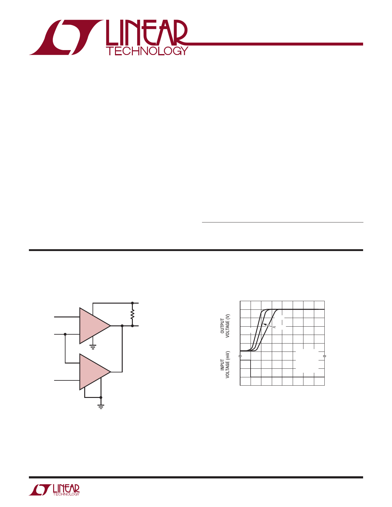
Response Time For Various Input Overdrives
6
5
4
3 20mV
2
1
0
100
50
0
2mV
5mV
VS = ±15V
VRL+
= 500Ω
+ = 5V
TA = 25°C
0 50 100 150 200 250 300 350
TIME (ns)
LT119/319 TA2
119a319afc
1
1 page 
TYPICAL PERFORMANCE CHARACTERISTICS
LT119A/LT319A
LM119/LM319
Output Saturation Voltage
25
TJ = 25°C
20
15
10
5
VS = ±15V
INPUT OVERDRIVE = 5mV
0
0 0.2 0.4 0.6 0.8 1.0
OUTPUT VOLTAGE (V)
LT119/319 G7
Supply Current
12
TJ = 25°C
10
8
POSITIVE SUPPLY
6
4 NEGATIVE SUPPLY
2
0
0 5 10 15 20
SUPPLY VOLTAGE (V)
LT119/319 G8
Output Limiting Characteristics
120
TJ = 25°C
100
SHORT-CIRCUIT CURRENT
AFTER 3 MINUTES
80
1.2
1.0
0.8
60 0.6
40
POWER DISSIPATION
20
0.4
0.2
00
0 5 10 15
OUTPUT VOLTAGE (V)
LT119/319 G9
Common Mode Limits
V+
–0.4 V+ = 5V, V– = 0V
–0.8 VS = ±15V
–1.2
–1.6
REFERRED TO SUPPLY VOLTAGES
–2.0
1.2
0.8 VS = ±15V, V+ = 5V, V– = 0V
0.4
V–
– 55 – 35 –15 5 25 45 65 85 105 125
TEMPERATURE (°C)
LT119/319 G10
Supply Current
12
10
POSITIVE SUPPLY = 15V
8
6 POSITIVE SUPPLY = 5V, V– = 0V
4
2 NEGATIVE SUPPLY = –15V
0
– 55 – 35 –15 5 25 45 65 85 105 125
TEMPERATURE (°C)
LT119/319 G11
TYPICAL APPLICATIONS
Relay Driver
5V 28V
INPUTS
10 – 11
1/2 LT319A 7
9+ 8
6
35V
LT119/319 TA3
High Noise Immunity 60Hz Sync Circuit
5V
68k
60Hz
INPUT
10VP-P
(TYP)
1N4148
20k
10 –
11
0.15µF
1/2 LT319A
9+ 8
6
7
3.3k
OUTPUT
10k
10k
LT119/319 TA4
119a319afc
5
5 Page 
REVISION HISTORY (Revision history begins at Rev C)
REV DATE DESCRIPTION
C 3/12 VSAT Conditions corrected from VIN ≤ 6mA to VIN ≤ 6mV
LT119A/LT319A
LM119/LM319
PAGE NUMBER
3
Information furnished by Linear Technology Corporation is believed to be accurate and reliable.
However, no responsibility is assumed for its use. Linear Technology Corporation makes no representa-
tion that the interconnection of its circuits as described herein will not infringe on existing patent rights.
119a319afc
11
11 Page | ||
| Páginas | Total 12 Páginas | |
| PDF Descargar | [ Datasheet LM319.PDF ] | |
Hoja de datos destacado
| Número de pieza | Descripción | Fabricantes |
| LM310 | Voltage Follower | National Semiconductor |
| LM3100 | LM3100 SIMPLE SWITCHER Synchronous 1MHz 1.5A Step-Down Voltage Regulator (Rev. G) | Texas Instruments |
| LM3100 | Voltage Regulator | National Semiconductor |
| LM3102 | LM3102/-Q1 SIMPLE SWITCHER Synchronous 1-MHz 2.5-A Step-Down Voltage Regulator (Rev. H) | Texas Instruments |
| Número de pieza | Descripción | Fabricantes |
| SLA6805M | High Voltage 3 phase Motor Driver IC. |
Sanken |
| SDC1742 | 12- and 14-Bit Hybrid Synchro / Resolver-to-Digital Converters. |
Analog Devices |
|
DataSheet.es es una pagina web que funciona como un repositorio de manuales o hoja de datos de muchos de los productos más populares, |
| DataSheet.es | 2020 | Privacy Policy | Contacto | Buscar |