|
|
PDF LTC1422 Data sheet ( Hoja de datos )
| Número de pieza | LTC1422 | |
| Descripción | Hot Swap Controller | |
| Fabricantes | Linear Technology | |
| Logotipo |  |
|
Hay una vista previa y un enlace de descarga de LTC1422 (archivo pdf) en la parte inferior de esta página. Total 16 Páginas | ||
|
No Preview Available !
LTC1422
Hot Swap Controller
FEATURES
s Allows Safe Board Insertion and Removal
from a Live Backplane
s System Reset Output with Programmable Delay
s Programmable Electronic Circuit Breaker
s User-Programmable Supply Voltage Power-Up Rate
s High Side Driver for an External N-Channel FET
s Controls Supply Voltages from 2.7V to 12V
s Undervoltage Lockout
s Soft Reset Input
s Glitch Filter on RESET
U
APPLICATIO S
s Hot Board Insertion
s Electronic Circuit Breaker
DESCRIPTIO
The LTC®1422 is an 8-pin Hot SwapTM controller that
allows a board to be safely inserted and removed from a
live backplane. Using an external N-channel pass transis-
tor, the board supply voltage can be ramped up at a
programmable rate. A high side switch driver controls the
N-channel gate for supply voltages ranging from 2.7V to
12V.
A programmable electronic circuit breaker protects
against shorts. The RESET output can be used to generate
a system reset when the supply voltage falls below a
programmable voltage. The ON pin can be used to cycle
the board power or to generate a soft reset.
The LTC1422 is available in 8-pin PDIP and SO packages.
, LTC and LT are registered trademarks of Linear Technology Corporation.
Hot Swap is a trademark of Linear Technology Corporation.
TYPICAL APPLICATIO
5V Hot Swap
R1 Q1
0.005Ω MTB50N06V
VCC
ON/RESET
GND
R2
10Ω
5%
8 76
2 VCC
SENSE GATE
5
ON FB
LTC1422
1
RESET
TIMER GND
3
C2
4
0.33µF
BACKPLANE PLUG-IN CARD
C1
0.1µF
R3
6.81k
1%
+
VOUT
5V
CLOAD
R4
2.43k
1%
µP
RESET
1422 TA01
1
1 page 
LTC1422
TYPICAL PERFORMANCE CHARACTERISTICS
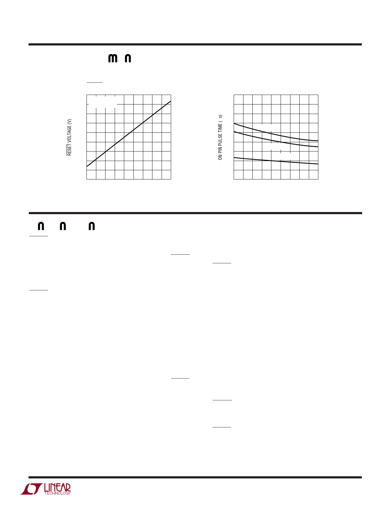
RESET Voltage vs Temperature
0.24
VCC = 5V
0.22 3mA PULL-UP
0.20
0.18
0.16
0.14
0.12
0.10
0.08
0.06
– 55 – 35 –15 5 25 45 65 85 105 125
TEMPERATURE (°C)
1422 G19
ON Pin Pulse (Soft Reset) Time
vs Temperature
55
50
45
40
VCC = 3V
35
30
VCC = 5V
25
20 VCC = 12V
15
10
– 55 – 35 –15 5 25 45 65 85 105 125
TEMPERATURE (°C)
1422 G20
PIN FUNCTIONS
RESET (Pin 1) : Open drain output to GND with a 12µA
pull-up to VCC. This pin is pulled low when the voltage at
the FB (Pin 5) goes below the FB pin threshold. The RESET
pin will go high one timing cycle after the voltage at the FB
pin goes above the FB pin threshold. An external pull-up
resistor can be used to speed up the rising edge on the
RESET pin or pull the pin to a voltage higher or lower than
VCC.
ON (Pin 2): Analog Input Pin. The threshold is set at 1.30V
with 80mV hysteresis. When the ON pin is pulled high, the
timer turns on for one cycle, then the charge pump turns
on. When the ON pin is pulled low longer than 40µs, the
GATE pin will be pulled low and remain off until the ON pin
is pulled high.
If the ON pin is pulled low for less than 15µs a soft reset
will occur. The charge pump remains on, and the RESET
pin is pulled low for one timing cycle starting 30µs from
the falling edge of the ON pin.
The ON pin is also used to reset the electronic circuit
breaker. If the ON pin is cycled low and high following the
trip of the circuit breaker, the circuit breaker is reset and
a normal power-up sequence will occur.
TIMER (Pin 3): Analog system timing generator pin. This
pin is used to set the delay before the charge pump turns
on after the ON pin goes high. It also sets the delay before
the RESET pin goes high, after the output supply voltage
is good, as sensed by the FB pin.
When the timer is off, an internal N-channel shorts the
TIMER pin to ground. When the timer is turned on, a 2µA
current from VCC is connected to the TIMER pin and the
voltage starts to ramp up with a slope given by: dV/dt =
2µA/CTIMER. When the voltage reaches the trip point
(1.232V), the timer will be reset by pulling the TIMER pin
back to ground. The timer period is given by: (1.232V •
CTIMER )/2µA.
GND (Pin 4): Chip Ground.
FB (Pin 5): Analog comparator input used to monitor the
output supply voltage with an external resistive divider.
When the voltage on the FB pin is lower than the 1.232V,
the RESET pin will be pulled low. An internal filter helps
prevent negative voltage glitches from triggering a reset.
When the voltage on the FB pin rises above the trip point,
the RESET pin will go high after one timing cycle.
5
5 Page 
LTC1422
APPLICATIONS INFORMATION
Since the pass transistor is in a common source configu-
ration, care must be taken to limit the inrush current into
capacitor C3. One way is to precharge C3 using resistor
R4. As the input supply is ramping up, current is flowing
through R4 and charging the capacitor C3. Once the input
supply crosses 38V, there is a timing cycle followed by the
ramp-up of the GATE pin. By this time the capacitor C3 is
sufficiently charged, thereby limiting the inrush current.
Another method to limit the inrush current is to slow down
the ramp-up rate of the GATE pin.
Hot Swapping 48V DC/DC Module with
Active High On/Off Control Signal
This application is identical to the previous except for the
polarity of the module’s on/off signal. The polarity reversal
is accomplished by transistor Q3 in Figure 13.
Hot Swapping Redundant 48V
In critical situations, redundant input supplies are neces-
sary. In Figure 14 a redundant 48V input is switched to a
power module. Supplies 1 and 2 are wire OR’ed using two
diodes D2 and D3. This results in the most negative of
these two supplies being used to drive the power module.
If one of the supplies is disconnected or a fuse opens, the
fault signal will be activated via diodes D4 and D5 and the
reset comparator at the FB pin. The GATE IN signal on the
Vicor module is controlled using the high voltage PNP Q2.
Once the module’s minus input pin is more negative than
the base of Q2 plus a diode drop, Q2 will turn off and the
module will turn on. This occurs when the source of Q1
plus a Zener voltage (D1) is more positive than the drain
of Q1 (in other words, when the switching FET Q1 has only
7.5V across its drain source).
Hot Swapping 48V Module with Isolated Controller
A power supervisory controller will sometimes reside on
an isolated supply with responsibility for other supplies.
Figure 15 shows how to Hot Swap a controller’s 5V supply
and a 48V module using two LTC1422s. Assuming the 5V
supply comes up first, the controller waits for a power
good signal from the 48V circuit. Once it receives the right
signals the controller activates the GATE IN pin of the Vicor
power module.
Power Supply Sequencer
A circuit that forces two supply voltages to power up
together is shown in Figure 16. The input supply voltages
may power up in any sequence, but both input voltages
must be within tolerance before Q1 and Q2 turn on. Back-
to-back transistors Q1 and Q2 ensure isolation between
the two supplies.
When the 5V input powers up before 3.3V, Q1 and Q2
remain off and the 5V output remains off until the 3.3V
input is within tolerance as sensed by resistors R1 and R2.
When the 3.3V input powers up before 5V, the diode D1
will pull up the 5V supply output with it. Once the 5V input
powers up and is within tolerance as sensed by R4 and R5,
Q1 and Q2 will turn on in about 1ms and pull the 5V output
up to its final voltage.
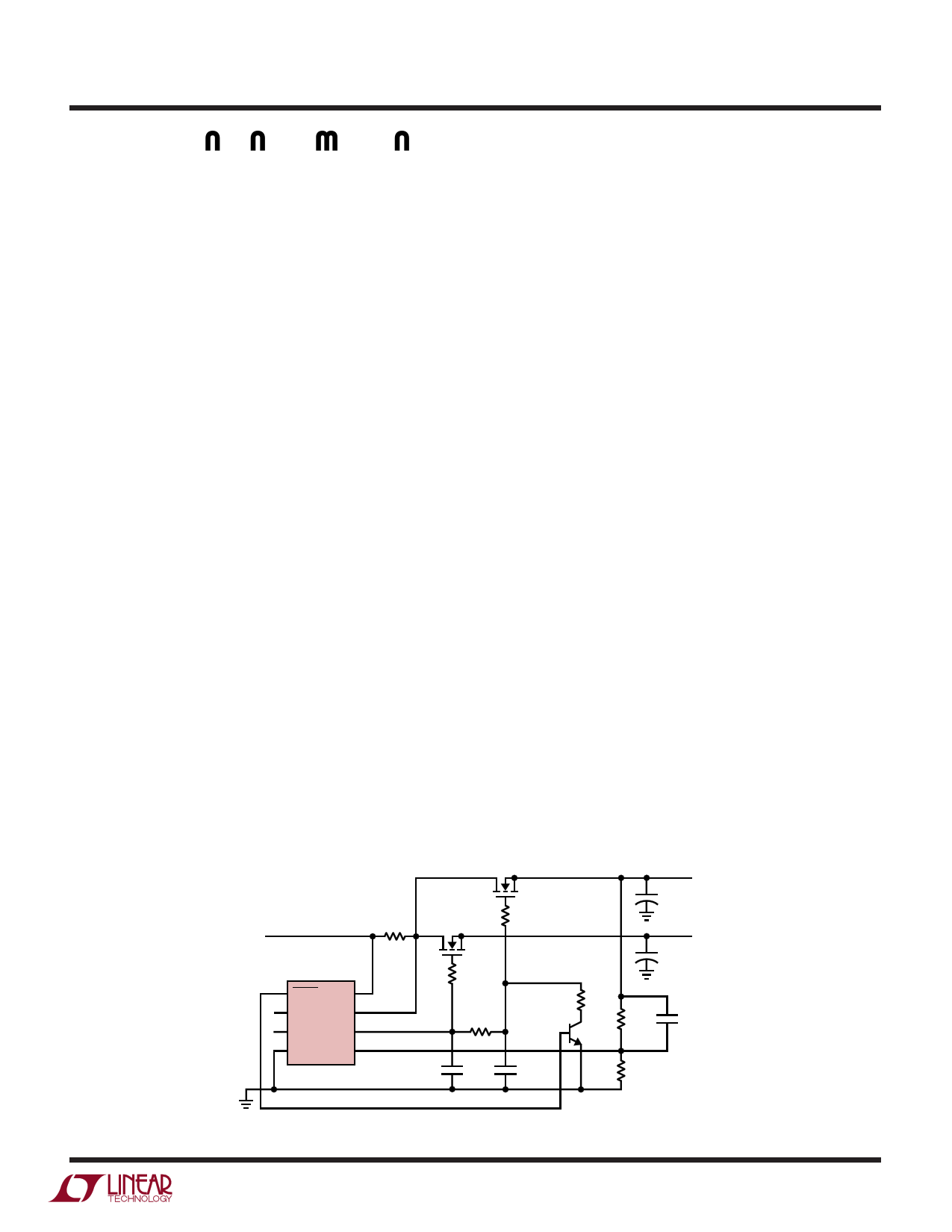
Q2
MMFT2N02ELT1
VIN CURRENT LIMIT: 2.5A
5V
LTC1422
1 RESET VCC 8
2 ON SENSE 7
3 TIMER GATE 6
4 GND
FB 5
R1
0.02Ω
Q1
5% MMFT2N02ELT1
R3
10Ω
5%
R6
1.6M
5%
C2
0.1µF
16V
R2
10Ω
5%
C1
0.0033µF
16V
VOUT
+ 3.3V
CLOAD
VOUT
+ 5V
CLOAD
R7
360k
5%
Q3
PN2222
R4
2.74k
1%
R5
1.62k
1%
C3
0.1µF
16V
Figure 11. Switching 5V and Generating 3.3V
1422 F11
11
11 Page | ||
| Páginas | Total 16 Páginas | |
| PDF Descargar | [ Datasheet LTC1422.PDF ] | |
Hoja de datos destacado
| Número de pieza | Descripción | Fabricantes |
| LTC1420 | 12-Bit/ 10Msps/ Sampling ADC | Linear Technology |
| LTC1420C | 12-Bit/ 10Msps/ Sampling ADC | Linear Technology |
| LTC1420CGN | 12-Bit/ 10Msps/ Sampling ADC | Linear Technology |
| LTC1420I | 12-Bit/ 10Msps/ Sampling ADC | Linear Technology |
| Número de pieza | Descripción | Fabricantes |
| SLA6805M | High Voltage 3 phase Motor Driver IC. |
Sanken |
| SDC1742 | 12- and 14-Bit Hybrid Synchro / Resolver-to-Digital Converters. |
Analog Devices |
|
DataSheet.es es una pagina web que funciona como un repositorio de manuales o hoja de datos de muchos de los productos más populares, |
| DataSheet.es | 2020 | Privacy Policy | Contacto | Buscar |
