|
|
|
PDF LTC1061AC Data sheet ( Hoja de datos )
| Número de pieza | LTC1061AC | |
| Descripción | High Performance Triple Universal Filter Building Block | |
| Fabricantes | Linear Technology | |
| Logotipo | ||
Hay una vista previa y un enlace de descarga de LTC1061AC (archivo pdf) en la parte inferior de esta página. Total 16 Páginas | ||
|
No Preview Available !
LTC1061
High Performance Triple
Universal Filter Building Block
FEATURES
s Up to 6th Order Filter Functions with a Single 20-Pin
0.3" Wide Package
s Center Frequency Range up to 35kHz
s fO × Q Product up to 1MHz
s Guaranteed Center Frequency and Q Accuracy Over
Temperature
s Guaranteed Low Offset Voltages Over Temperature
s 90dB Signal-to-Noise Ratio
s Filter Operates from Single 4.7V Supply and up to
±8V Supplies
s Guaranteed Filter Specifications with ±5V Supply and
±2.37V Supply
s Low Power Consumption with Single 5V Supply
s Clock Inputs T2L and CMOS Compatible
APPLICATI S
s High Order, Wide Frequency Range Bandpass,
Lowpass, Notch Filters
s Low Power Consumption, Single 5V Supply,
Clock-Tunable Filters
s Tracking Filters
s Antialiasing Filters
LTCMOSTM is a trademark of Linear Technology Corp.
DESCRIPTIO
The LTC1061 consists of three high performance, univer-
sal filter building blocks. Each filter building block together
with an external clock and 2 to 5 resistors can produce
various second order functions which are available at its
three output pins. Two out of three always provide low-
pass and bandpass functions while the third output pin
can produce highpass or notch or allpass. The center
frequency of these functions can be tuned with an external
clock or an external clock and a resistor ratio. For Q < 5, the
center frequency ranges from 0.1Hz to 35kHz. For Qs of 10
or above, the center frequency ranges from 0.1Hz to
28kHz.
The LTC1061 can be used with single or dual supplies
ranging from ±2.37V to ±8V (or 4.74V to 16V). When the
filter operates with supplies of ±5V and above, it can
handle input frequencies up to 100kHz.
The LTC1061 is compatible with the LTC1059 single
universal filter and the LTC1060 dual. Higher than 6th
order functions can be obtained by cascading the LTC1061
with the LTC1059 or LTC1060. Any classical filter realiza-
tion can be obtained.
The LTC1061 is manufactured by using Linear Technology’s
enhanced LTCMOSTM silicon gate process.
TYPICAL APPLICATI
6th Order, Clock-Tunable, 0.5dB Ripple Chebyshev BP Filter
9.31k
165k
VIN < 100kHz
1k
165k
4.99k
7.5V
T2 CLK IN < 1.2MHz
1 20
2 19 78.7k
3 18 4.99k
4 17 23.7k
5 16
LTC1061
6 15 V– = –7.5V
7 14 4.99k
8 13 165k
9 12 5.49k
49.9k
V+ = 7.5V
10
11
VOUT
1061 TA01
Amplitude Response
2kHz
0
fCLK = 1MHz
–20
–40
–60
–80
–100
0
10 20 30 40 50
INPUT FREQUENCY GAIN (kHz)
LTC1061 • TA02
1
1 page 
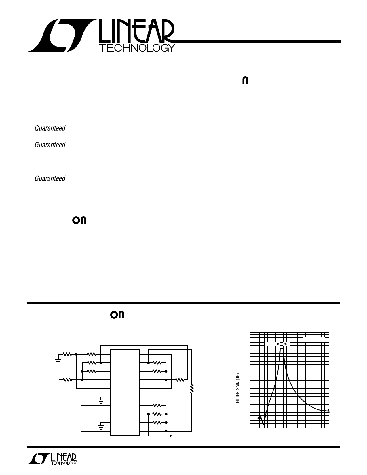
BLOCK DIAGRA S
CLK
(8)
LEVEL
SHIFT
CLOCK
GENERATOR
INVA
(4)
TO FILTER A
–
+
LEVEL
SHIFT
CLOCK
GENERATOR
INVB
(17)
TO FILTER B
–
+
LEVEL
SHIFT
CLOCK
GENERATOR
INVC
(11)
TO FILTER C
–
+
LTC1061
NA BPA LPA
(3) (2) (1)
+ Σ +∫
–
+∫
S1A
(5)
NB
(18)
BPB LPB
(19) (20)
+ Σ +∫
–
+∫
S1B
(16)
HPC BPC LPC
(12) (13) (14)
+∫ +∫
LEVEL SHIFT
(9)
50/100/
HOLD
(7)
AGND
(6)
V+
(10)
V–
(15)
1061 BD
U UU
UU
PI DESCRIPTIO A D APPLICATIO HI TS
Power Supplies (Pins 10, 15)
They should be bypassed with 0.1µF disc ceramic. Low
noise, nonswitching, power supplies are recommended.
The device operates with a single 5V supply, Figure 1, and
with dual supplies. The absolute maximum operating
power supply voltage is ±9V.
Clock and Level shift (Pins 8, 9)
frequencies below 500kHz the clock “on” time can be as
low as 300ns. The maximum clock frequency for ±5V
supplies and above is 2.4MHz.
S1A, S1B (Pins 5, 16)
These are voltage input pins. If used, they should be driven
with a source impedance below 5kΩ. when they are not
used, they should be tied to the analog ground Pin 6.
When the LTC1061 operates with symmetrical dual sup-
plies the level shift Pin 9 should be tied to analog ground.
For single 5V supply operation, the level shift pin should be
tied to Pin 15 which will be the system ground. The typical
logic threshold levels of the clock pin are as follows: 1.65V
above the level shift pin for ±5V supply operation, 1.75V
for ±7.5V and above, and 1.4V for single 5V supply
operation. The logic threshold levels vary ±100mV over
the full military temperature range. The recommended
duty cycle of the input clock is 50% although for clock
AGND (Pin 6)
When the LTC1061 operates with dual supplies, Pin 6
should be tied to system ground. When the LTC1061
operates with a single positive supply, the analog ground
pin should be tied to 1/2 supply, Figure 1. The positive
input of all the internal op amps, as well as the common
reference of all the internal switches, are internally tied to
the analog ground pin. Because of this, a “clean” ground
is recommended.
5
5 Page 
WU
ODES OF OPERATIO
LTC1061
STANDARD 1%
0 RESISTOR VALUES
–10
R11 = 39.2k
R31 = 13.7k
R21 = 10k
R41 = 39.2k
–20
Rh1 = 20.5k
Rl1 = 12.4k
R22 = 10k
R32 = 26.7k
–30
R42 = 14k
Rh2 = 32.4k
–40
Rl2 = 11.8k
R33 = 100k
R23 = 10k
–50 NOTES: USE A 10pF ACROSS R42
–60
FOR fCLK > 1MHz.
THE ELLIPTIC LOWPASS FILTER
–70 HAS ONLY TWO NOTCHES IN THE
STOPBAND, AND IT OPERATES
–80 WITH A CLOCK TO CUTOFF
–90 FREQUENCY RATIO OF 50:1.
0 1 2 3 4 5 6 7 8 9 10
fIN (kHz)
1061 F15
Figure 15. Resistor Values and Amplitude Response of
the Topology of Figure 12.
passive ladder filters provide enough data to synthesize
the above filters. The measured amplitude response of
such a lowpass is shown in Figure 15 where the filter
output is taken out of side A’s Pin 1, Figure 12. The clock-
to-center frequency ratio can be either 50:1 or 100:1
because the last stage of the LTC1061 operates in Mode 1
with a center frequency very close to the overall cutoff
frequency of the lowpass filter.
In Figure 16, all three sides of the LTC1061 are connected
in Mode 3a. This topology is useful for elliptic highpass
and notch filters with clock-to-cutoff (or notch) frequency
ratio higher than 100:1. This is often required to extend the
allowed input signal frequency range and to avoid prema-
ture aliasing. Figure 16 is also a versatile, general purpose
architecture providing 3 notches and 4 pole pairs, and
there is no restriction on the location of the poles with
respect to the notch frequencies. The drawbacks, when
compared to Figure 12, are the use of an external op amp
and the increased number of the required external resis-
tors.
Figure 17 shows the measured frequency of a 6th order
highpass elliptic filter operating with 250:1 clock-to-cutoff
frequency ratio. With a 1MHz clock, for instance, the filter
yields a 4kHz cutoff frequency, thus allowing an input
frequency range beyond 100kHz. Band limiting can be
easily added by placing a capacitor across the feedback
resistor of the external op amp of Figure 16.
Rg
–
Rh3
Rl3
LT1056
+
VOUT
R43
R33
R23
T2Ll, CMOS
CLOCK INPUT
V+
VIN
1 20
2 19
3 18
4 17
5 16
LTC1061
6 15
7 14
8 13
9 12
10 11
Rl2
R42
R32
R22
Rh2
V – Rl1
R41
R31
R21
Rh1
R11
LTC1061 F16
Figure 16. Using an External Op Amp to Connect
all 3 Sides of the LTC1061 in Mode 3a.
0 fCLK = 250kHz
STANDARD 1%
RESISTOR VALUES
–10
–20
–30
–40
–50
–60
–70
–80
–90
0
R11 = 105k
R31 = 47.5k
Rh1 = 10k
R22 = 32.4k
R42 = 52.3k
Rl2 = 750k
R33 = 255k
Rh3 = 10k
Rg = 140k
R21 = 10k
R41 = 45.3k
Rl1 = 1.07M
R32 = 28.7k
Rh2 = 42.2k
R23 = 10k
R43 = 63.4k
Rl3 = 110k
NOTE: FOR CLOCK FREQUENCIES
BELOW 500kHz, USE A CAPACI-
TOR IN PARALLEL WITH R21
SUCH AS (1/2πR21C) ≅ fCLK/3.
0.5 1.0 1.5 2.0 2.5
fIN (kHz)
1061 F17
Figure 17. Measured Amplitude Response of the Topology of
Figure 16, Configured to Provide a 6th Order Elliptic Highpass
Filter Operating with a Clock-to-Cutoff Frequency Ratio of 250:1.
11
11 Page | ||
| Páginas | Total 16 Páginas | |
| PDF Descargar | [ Datasheet LTC1061AC.PDF ] | |
Hoja de datos destacado
| Número de pieza | Descripción | Fabricantes |
| LTC1061AC | High Performance Triple Universal Filter Building Block | Linear Technology |
| LTC1061ACJ | High Performance Triple Universal Filter Building Block | Linear Technology |
| LTC1061ACN | High Performance Triple Universal Filter Building Block | Linear Technology |
| LTC1061AM | High Performance Triple Universal Filter Building Block | Linear Technology |
| Número de pieza | Descripción | Fabricantes |
| SLA6805M | High Voltage 3 phase Motor Driver IC. |
Sanken |
| SDC1742 | 12- and 14-Bit Hybrid Synchro / Resolver-to-Digital Converters. |
Analog Devices |
|
DataSheet.es es una pagina web que funciona como un repositorio de manuales o hoja de datos de muchos de los productos más populares, |
| DataSheet.es | 2020 | Privacy Policy | Contacto | Buscar |