|
|
|
PDF MAX4662EPE Data sheet ( Hoja de datos )
| Número de pieza | MAX4662EPE | |
| Descripción | 2.5W / Quad / SPST / CMOS Analog Switches | |
| Fabricantes | Maxim Integrated | |
| Logotipo | ||
Hay una vista previa y un enlace de descarga de MAX4662EPE (archivo pdf) en la parte inferior de esta página. Total 12 Páginas | ||
|
No Preview Available !
19-1516; Rev 0; 7/99
2.5Ω, Quad, SPST,
CMOS Analog Switches
General Description
The MAX4661/MAX4662/MAX4663 quad analog switches
feature low on-resistance of 2.5Ω max. On-resistance is
matched between switches to 0.5Ω max and is flat
(0.5Ω max) over the specified signal range. Each
switch can handle Rail-to-Rail® analog signals. Off-
leakage current is only 5nA max at TA = +85°C. These
analog switches are ideal in low-distortion applications
and are the preferred solution over mechanical relays in
automatic test equipment or applications where current
switching is required. They have lower power require-
ments, use less board space, and are more reliable
than mechanical relays.
The MAX4661 has four normally closed (NC) switches,
and the MAX4662 has four normally open (NO) switches.
The MAX4663 has two NC and two NO switches, and fea-
tures guaranteed break-before-make switching.
These devices operate from a single +4.5V to +36V sup-
ply or from dual ±4.5V to ±20V supplies. A separate logic
supply pin guarantees TTL/CMOS-logic compatibility
when operating across the entire supply voltage range.
Applications
Reed Relay Replacement Avionics
Test Equipment
ADC Systems
Communication Systems Sample-and-Hold Circuits
PBX, PABX Systems
Data Acquisition Systems
Audio-Signal Routing
Features
o Low On-Resistance (2.5Ω max)
o Guaranteed RON Match Between Channels
(0.5Ω max)
o Guaranteed RON Flatness over Specified Signal
Range (0.5Ω max)
o Rail-to-Rail Signal Handling
o Guaranteed Break-Before-Make (MAX4663)
o > 2kV ESD Protection per Method 3015.7
o +4.5V to +36V Single-Supply Operation
±4.5V to ±20V Dual-Supply Operation
o TTL/CMOS-Compatible Control Inputs
Ordering Information
PART
TEMP. RANGE PIN-PACKAGE
MAX4661CAE
0°C to +70°C
16 SSOP
MAX4661CWE
0°C to +70°C
16 Wide SO
MAX4661CPE
0°C to +70°C
16 Plastic DIP
MAX4661EAE
MAX4661EWE
MAX4661EPE
-40°C to +85°C
-40°C to +85°C
-40°C to +85°C
16 SSOP
16 Wide SO
16 Plastic DIP
Ordering Information continued at end of data sheet.
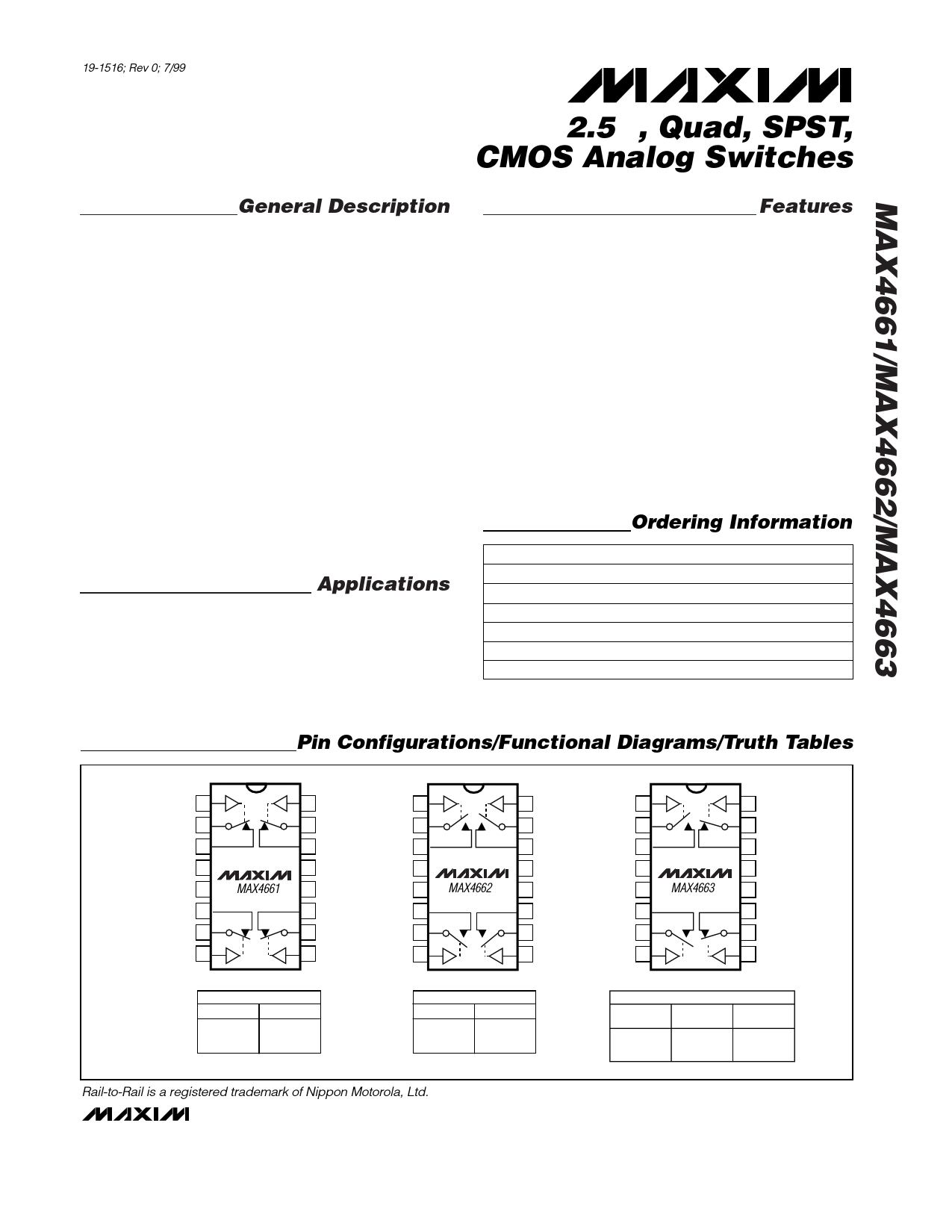
Pin Configurations/Functional Diagrams/Truth Tables
TOP VIEW
IN1 1
COM1 2
NC1 3
V- 4
GND 5
NC4 6
COM4 7
IN4 8
MAX4661
16 IN2
15 COM2
14 NC2
13 V+
12 VL
11 NC3
10 COM3
9 IN3
IN1 1
COM1 2
NO1 3
V- 4
GND 5
NO4 6
COM4 7
IN4 8
MAX4662
16 IN2
15 COM2
14 NO2
13 V+
12 VL
11 NO3
10 COM3
9 IN3
IN1 1
COM1 2
NO1 3
V- 4
GND 5
NO4 6
COM4 7
IN4 8
MAX4663
16 IN2
15 COM2
14 NC2
13 V+
12 VL
11 NC3
10 COM3
9 IN3
SSOP/SO/DIP
MAX4661
LOGIC
SWITCH
0 ON
1 OFF
SSOP/SO/DIP
MAX4662
LOGIC
SWITCH
0 OFF
1 ON
SWITCHES SHOWN FOR LOGIC “0” INPUT
SSOP/SO/DIP
MAX4663
LOGIC
SWITCHES SWITCHES
1, 4 2, 3
0 OFF ON
1 ON OFF
Rail-to-Rail is a registered trademark of Nippon Motorola, Ltd.
________________________________________________________________ Maxim Integrated Products 1
For free samples & the latest literature: http://www.maxim-ic.com, or phone 1-800-998-8800.
For small orders, phone 1-800-835-8769.
1 page 
2.5Ω, Quad, SPST,
CMOS Analog Switches
ELECTRICAL CHARACTERISTICS—Single Supply (continued)
(V+ = +12V, V- = 0, VL = +5V, VIN_H = +2.4V, VIN_L = +0.8V, TA = TMIN to TMAX, unless otherwise noted. Typical values are at
TA = +25°C.) (Note 2)
PARAMETER
SYMBOL
CONDITIONS
MIN TYP MAX UNITS
SWITCH DYNAMIC CHARACTERISTICS
Turn-On Time (Note 3)
Turn-Off Time (Note 3)
tON
VCOM_ = 10V,
Figure 2
tOFF
VCOM_ = 10V,
Figure 2
TA = +25°C
TA = TMIN to TMAX
TA = +25°C
TA = TMIN to TMAX
200 400
500
100 250
350
ns
ns
Break-Before-Make Time
(MAX4663 only) (Note 3)
tOPEN
VCOM_ = 10V, Figure 3, TA = +25°C
5 125
ns
Charge Injection
Q
CL = 1.0nF, VGEN = 0, RGEN = 0,
Figure 4
20 pC
Crosstalk (Note 8)
NC_ or NO_ Capacitance
COM Off-Capacitance
On-Capacitance
VCT
COFF
CCOM
CCOM
RL = 50Ω, CL = 5pF, f = 1MHz,
Figure 6
f = 1MHz, Figure 7
f = 1MHz, Figure 7
f = 1MHz, Figure 8
-60 dB
85 pF
85 pF
140 pF
Note 2: The algebraic convention, where the most negative value is a minimum and the most positive value a maximum, is used in
this data sheet.
Note 3: Guaranteed by design.
Note 4: ∆RON = RON(MAX) - RON(MIN).
Note 5: Flatness is defined as the difference between the maximum and minimum value of on-resistance as measured over the
specified analog signal range.
Note 6: Leakage parameters are 100% tested at maximum-rated hot temperature and guaranteed by correlation at +25°C.
Note 7: Off-isolation = 20log10 [VCOM / (VNC or VNO)], VCOM = output, VNC or VNO = input to off switch.
Note 8: Between any two switches.
Note 9: Leakage testing at single supply is guaranteed by testing with dual supplies.
_______________________________________________________________________________________ 5
5 Page 
2.5Ω, Quad, SPST,
CMOS Analog Switches
Package Information
______________________________________________________________________________________ 11
11 Page | ||
| Páginas | Total 12 Páginas | |
| PDF Descargar | [ Datasheet MAX4662EPE.PDF ] | |
Hoja de datos destacado
| Número de pieza | Descripción | Fabricantes |
| MAX4662EPE | 2.5W / Quad / SPST / CMOS Analog Switches | Maxim Integrated |
| Número de pieza | Descripción | Fabricantes |
| SLA6805M | High Voltage 3 phase Motor Driver IC. |
Sanken |
| SDC1742 | 12- and 14-Bit Hybrid Synchro / Resolver-to-Digital Converters. |
Analog Devices |
|
DataSheet.es es una pagina web que funciona como un repositorio de manuales o hoja de datos de muchos de los productos más populares, |
| DataSheet.es | 2020 | Privacy Policy | Contacto | Buscar |