|
|
PDF TP3070V Data sheet ( Hoja de datos )
| Número de pieza | TP3070V | |
| Descripción | COMBO II Programmable PCM CODEC/Filter | |
| Fabricantes | National Semiconductor | |
| Logotipo | ||
Hay una vista previa y un enlace de descarga de TP3070V (archivo pdf) en la parte inferior de esta página. Total 26 Páginas | ||
|
No Preview Available !
April 1994
TP3070, TP3071, TP3070-X
COMBO® II Programmable PCM CODEC/Filter
General Description
The TP3070 and TP3071 are second-generation combined
PCM CODEC and Filter devices optimized for digital switch-
ing applications on subscriber line and trunk cards. Using
advanced switched capacitor techniques, COMBO II com-
bines transmit bandpass and receive lowpass channel filters
with a companding PCM encoder and decoder. The devices
are A-law and µ-law selectable and employ a conventional
serial PCM interface capable of being clocked up to
4.096 MHz. A number of programmable functions may be
controlled via a serial control port.
Channel gains are programmable over a 25.4 dB range in
each direction, and a programmable filter is included to en-
able Hybrid Balancing to be adjusted to suit a wide range of
loop impedance conditions. Both transformer and active
SLIC interface circuits with real or complex termination im-
pedances can be balanced by this filter, with cancellation in
excess of 30 dB being readily achievable when measured
across the passband against standard test termination net-
works.
To enable COMBO II to interface to the SLIC control leads, a
number of programmable latches are included; each may be
configured as either an input or an output. The TP3070 pro-
vides 6 latches and the TP3071 5 latches.
Features
n Complete CODEC and FILTER system including:
— Transmit and receive PCM channel filters
— µ-law or A-law companding encoder and decoder
— Receive power amplifier drives 300Ω
— 4.096 MHz serial PCM data (max)
n Programmable Functions:
— Transmit gain: 25.4 dB range, 0.1 dB steps
— Receive gain: 25.4 dB range, 0.1 dB steps
— Hybrid balance cancellation filter
— Time-slot assignment; up to 64 slots/frame
— 2 port assignment (TP3070)
— 6 interface latches (TP3070)
— A or µ-law
— Analog loopback
— Digital loopback
n Direct interface to solid-state SLICs
n Simplifies transformer SLIC; single winding secondary
n Standard serial control interface
n 80 mW operating power (typ)
n 1.5 mW standby power (typ)
n Designed for CCITT and LSSGR applications
n TTL and CMOS compatible digital interfaces
n Extended temperature versions available for −40˚C to
+85˚C (TP3070V-X)
Note: See also AN-614, COMBO II application guide.
COMBO® and TRI-STATE® are registered trademarks of National Semiconductor Corporation.
© 1999 National Semiconductor Corporation DS008635
www.national.com
1 page 
Functional Description (Continued)
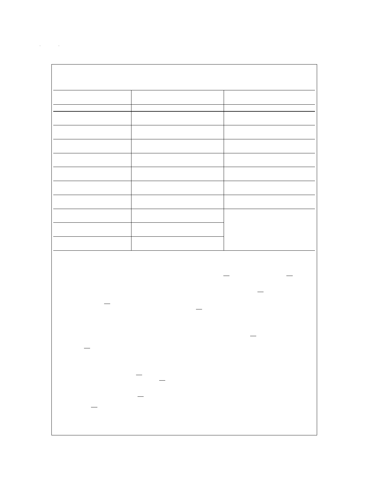
TABLE 1. Programmable Register Instructions
Function
Byte 1 (Note 1)
Byte 2 (Note 1)
76543210
76543210
Single Byte Power-Up/Down
PXXXXX0X
None
Write Control Register
P000001X
See Table 2
Read-Back Control Register
P000011X
See Table 2
Write to Interface Latch Register
P000101X
See Table 4
Read Interface Latch Register
P000111X
See Table 4
Write Latch Direction Register
P001001X
See Table 3
Read Latch Direction Register
P001011X
See Table 3
Write Receive Gain Register
P010001X
See Table 8
Read Receive Gain Register
P010011X
See Table 8
Write Transmit Gain Register
P010101X
See Table 7
Read Transmit Gain Register
P010111X
See Table 7
Write Receive Time-Slot/Port
P100101X
See Table 6
Read-Back Receive Time-Slot/Port
P100111X
See Table 6
Write Transmit Time-Slot/Port
P101001X
See Table 6
Read-Back Transmit Time-Slot/Port
P101011X
See Table 6
Write Hybrid Balance Register 1
Read Hybrid Balance Register 1
Write Hybrid Balance Register 2
Read Hybrid Balance Register 2
Write Hybrid Balance Register 3
Read Hybrid Balance Register 3
P011001X
P011011X
P011101X
P011111X
P100001X
P100011X
Derive from
Optimization
Routine in
TP3077SW
Program
Note 1: Bit 7 of bytes 1 and 2 is always the first bit clocked into or out from the CI, CO or CI/O pin. X = don’t care.
Note 2: “P” is the power-up/down control bit, see “Power-Up/Down Control” section. (“0” = Power Up, “1” = Power Down)
Note 3: Other register address codes are invalid and should not be used.
SERIAL CONTROL PORT
Control information and data are written into or read-back
from COMBO II via the serial control port consisting of the
control clock CCLK, the serial data input/output CI/O, (or
separate input, CI, and output, CO, on the TP3070 only), and
the Chip Select input, CS. All control instructions require 2
bytes, as listed in Table 1, with the exception of a single byte
power-up/down command. The byte 1 bits are used as fol-
lows: bit 7 specifies power up or power down; bits 6, 5, 4 and
3 specify the register address; bit 2 specifies whether the in-
struction is read or write; bit 1 specifies a one or two byte in-
struction; and bit 0 is not used.
To shift control data into COMBO II, CCLK must be pulsed 8
times while CS is low. Data on the CI/O (or CI) input is
shifted into the serial input register on the falling edge of
each CCLK pulse. After all data is shifted in, the contents of
the input shift register are decoded, and may indicate that a
2nd byte of control data will follow. This second byte may ei-
ther be defined by a second byte-wide CS pulse or may fol-
low the first contiguously, i.e. it is not mandatory for CS to re-
turn high between the first and second control bytes. At the
end of CCLK8 in the 2nd control byte the data is loaded into
the appropriate programmable register. CS may remain low
continuously when programming successive registers, if de-
sired. However, CS should be set high when no data trans-
fers are in progress.
To readback Interface Latch data or status information from
COMBO II, the first byte of the appropriate instruction is
strobed in while CS is low, as defined in Table 1. CS must be
kept low, or be taken low again for a further 8 CCLK cycles,
during which the data is shifted onto the CO or CI/O pin on
the rising edges of CCLK. When CS is high the CO or CI/O
pin is in the high-impedance TRI-STATE, enabling the CI/O
pins of many devices to be multiplexed together.
If CS returns high during either byte 1 or byte 2 before all
eight CCLK pulses of that byte occur, both the bit count and
byte count are reset and register contents are not affected.
This prevents loss of synchronization in the control interface
as well as corruption of register data due to processor inter-
rupt or other problem. When CS returns low again, the de-
vice will be ready to accept bit 1 of byte 1 of a new instruc-
tion.
Programmable Functions
1.0 POWER-UP/DOWN CONTROL
Following power-on initialization, power-up and power-down
control may be accomplished by writing any of the control in-
structions listed in Table 1 into COMBO II with the “P” bit set
to “0” for power-up or “1” for power-down. Normally it is rec-
ommended that all programmable functions be initially pro-
grammed while the device is powered down. Power state
control can then be included with the last programming in-
struction or the separate single-byte instruction. Any of the
programmable registers may also be modified while the de-
5 www.national.com
5 Page 
Absolute Maximum Ratings (Note 9)
If Military/Aerospace specified devices are required,
please contact the National Semiconductor Sales Office/
Distributors for availability and specifications.
VCC to GND
Voltage at VFXI
Voltage at any Digital Input
7V
VCC + 0.5V to VBB − 0.5V
VCC + 0.5V to GND − 0.5V
Storage Temperature Range
VBB to GND
Current at VFR0
Current at any Digital Output
Lead Temperature
(Soldering, 10 sec.)
−65˚C to + 150˚C
−7V
±100 mA
±50 mA
300˚C
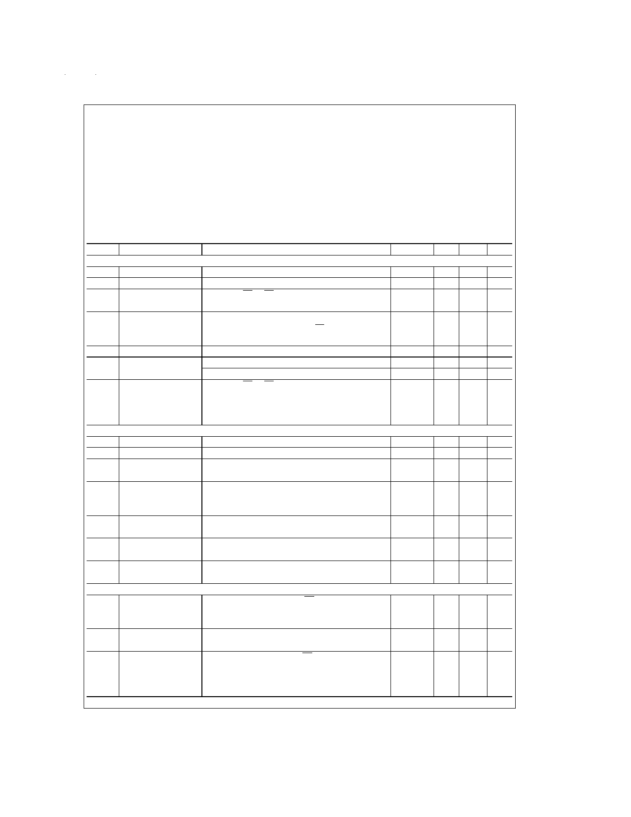
Electrical Characteristics
+U7n0le˚Css(o−t4h0e˚rCwitsoe+n8o5t˚eCd,folimr TitPs 3p0ri7n0te-Xd)inbyBcOoLrrDelacthioanrawctiethrs1a0r0e%guealercatnritceaeldtefosrtinVgCCat=TA+5=V2±55˚C%.,AVllBoBth=er−5limV it±s5a%re;
TA = 0˚C to
assured by
correlation with other production tests and/or product design and characterization. All signals referenced to GND. Typicals
specified at VCC = +5V, VBB = −5V, TA = 25˚C.
Symbol
Parameter
Conditions
Min Typ Max Units
DIGITAL INTERFACES
VIL Input Low Voltage All Digital Inputs (DC Meas.) (Note 10)
VIH Input High Voltage All Digital Inputs (DC Meas.) (Note 10)
VOL
Output Low Voltage
DX0, DX1, TSX0, TSX1 and CO, IL = 3.2 mA,
All Other Digital Outputs, IL = 1 mA
VOH
Output High Voltage
DX0, DX1 and CO, IL = −3.2 mA,
All Other Digital Outputs (except TSX), IL = −1 mA
All Digital Outputs, IL = −100 µA
IIL
Input Low Current
Any Digital Input, GND < VIN < VIL
IIH
Input High Current
Any Digital Input except MR, VIH < VIN < VCC
MR Only
2.0
2.4
VCC − 0.5
−10
−10
−10
0.7 V
V
0.4 V
V
V
10 µA
10 µA
100 µA
IOZ Output Current in
DX0, DX1, TSX0, TSX1, CO and CI/O (as an Output)
High Impedance
IL5–IL0 When Selected as Inputs
State (TRI-STATE)
GND < VOUT < VCC
−40˚C to +85˚C (TP3070-X)
−10
−30
10 µA
30 µA
ANALOG INTERFACES
IVFXI
RVFXI
VOSX
RLVFRO
Input Current, VFXI
Input Resistance
Input Offset Voltage
Applied at VFXI
Load Resistance
−3.3V < VFXI < 3.3V
−3.3V < VFXI < 3.3V
Transmit Gain = 0 dB
Transmit Gain = 25.4 dB
Receive Gain = 0 dB
Receive Gain = −0.5 dB
−10.0
390
15k
600
10.0 µA
620 kΩ
200 mV
10 mV
Ω
Receive Gain = −1.2 dB
300
CLVFRO Load Capacitance
ROVFRO Output Resistance
VOSR Output Offset
Voltage at VFRO
POWER DISSIPATION
RLVFRO ≥ 300Ω
CLVFRO from VFRO to GND
Steady Zero PCM Code Applied to
DR0 or DR1
Alternating ± Zero PCM Code Applied to
DR0 or DR1, Maximum Receive Gain
−200
200 pF
1.0 3.0
Ω
200 mV
ICC0
Power Down Current
CCLK, CI/O, CI, CO, = 0.4V, CS = 2.4V
Interface Latches Set as Outputs with No Load,
0.1 0.6 mA
All Other Inputs Active, Power Amp Disabled
IBB0 Power Down Current As Above
−40˚C to +85˚C (TP3070-X)
−0.1
−0.3
−0.4
mA
mA
ICC1
Power Up Current
CCLK, CI/O, CI, CO = 0.4V, CS = 2.4V
No Load on Power Amp
8.0 11.0 mA
Interface Latches Set as Outputs with No Load
−40˚C to +85˚C (TP3070-X)
13.0 mA
11 www.national.com
11 Page | ||
| Páginas | Total 26 Páginas | |
| PDF Descargar | [ Datasheet TP3070V.PDF ] | |
Hoja de datos destacado
| Número de pieza | Descripción | Fabricantes |
| TP3070 | COMBO II Programmable PCM CODEC/Filter | National Semiconductor |
| TP3070 | TP3070 TP3071 TP3070-X COMBO II Programmable PCM CODEC/Filter | Texas Instruments |
| TP3070-x | TP3070 TP3071 TP3070-X COMBO II Programmable PCM CODEC/Filter | Texas Instruments |
| TP3070V | COMBO II Programmable PCM CODEC/Filter | National Semiconductor |
| Número de pieza | Descripción | Fabricantes |
| SLA6805M | High Voltage 3 phase Motor Driver IC. |
Sanken |
| SDC1742 | 12- and 14-Bit Hybrid Synchro / Resolver-to-Digital Converters. |
Analog Devices |
|
DataSheet.es es una pagina web que funciona como un repositorio de manuales o hoja de datos de muchos de los productos más populares, |
| DataSheet.es | 2020 | Privacy Policy | Contacto | Buscar |
