|
|
|
PDF CXA1785 Data sheet ( Hoja de datos )
| Número de pieza | CXA1785 | |
| Descripción | US Audio Multiplexing Decoder | |
| Fabricantes | Sony Corporation | |
| Logotipo | ||
Hay una vista previa y un enlace de descarga de CXA1785 (archivo pdf) en la parte inferior de esta página. Total 29 Páginas | ||
|
No Preview Available !
CXA1785AR
RGB Decoder/Driver
For the availability of this product, please contact the sales office.
Description
The CXA1785AR is an RGB decoder/driver
designed to drive LCD panels. This IC converts
composite video signals, Y/C signals and Y/color
difference signals into RGB signals used for driving
LCDs.
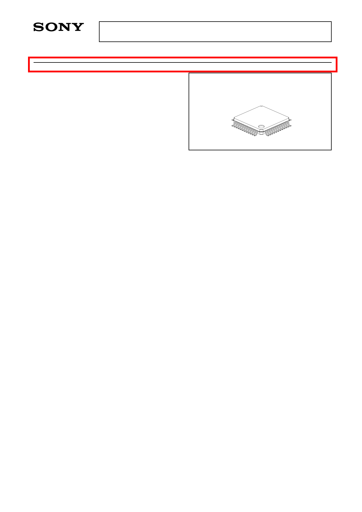
48 pin LQFP (Plastic)
Features
• Both NTSC/PAL compatible
• Supports composite inputs, Y/C inputs and Y/color
difference input
• Band pass filter, trap and delay line
• Sharpness function
• γ compensation circuit
• R, B output delay time adjustment circuit
• Polarity reverse circuit
Applications
• Color liquid crystal viewfinders
• Liquid crystal projectors
• Industrial monitors
Structure
Bipolar silicon monolithic IC
Absolute Maximum Ratings (Ta=25°C)
• Supply voltage
VCC1-GND
6
V
• Supply voltage
VCC2-VEE
15
V
• Supply voltage
GND-VEE
10
V
• Input pin voltage
VIN
VCC1
V
• Operating temperature Topr –30 to +85 °C
• Storage temperature Tstg –55 to +150 °C
• Allowable power dissipation
PD 560 mW
Operating Conditions
• Supply voltage
VCC1-GND 4.25 to 5.25
• Supply voltage
VCC2-GND 4.25 to 14.0
• Supply voltage
VCC2-VEE 11.25 to 14.0
• Supply voltage
VEE-GND –8.75 to 0
V
V
V
V
Sony reserves the right to change products and specifications without prior notice. This information does not convey any license by
any implication or otherwise under any patents or other right. Application circuits shown, if any, are typical examples illustrating the
operation of the devices. Sony cannot assume responsibility for any problems arising out of the use of these circuits.
—1—
E93Z28-TE
1 page 
CXA1785AR
Pin No. Symbol
12 CHROMA
OUT
Pin voltage
2.3V
Equivalent circuit
VCC1
Description
Color adjusted and burst taken
out chroma signal is output.
12
13 HUE
14 VXO IN
3.9V
VEE
VCC1
13
VEE
VCC1
GND
GND
Color phase adjustment pin.
Also doubles as the NTSC,
PAL or Y/color difference
switch. PAL is selected when
this pin is connected to GND;
Y/color difference is selected
when this pin is connected to
Vcc1.
VXO input.
Leave this pin open for Y/color
difference input.
15 APC
FILTER
14
VEE
VCC1
15
GND
APC detection filter connection.
Leave this pin open for Y/color
difference input.
16 VXO OUT
2.7V
VEE
VCC1
16
GND
VXO output.
Leave this pin open for Y/color
difference input.
17 GND
18 VEE
VEE GND
Ground.
Minimum electric potential con-
nection.
—5—
5 Page 
CXA1785AR
Item Symbol
Conditions
Min. Typ.
Amount of image quality Gp5 SW5→a, SW46→ON
14.0 17.0
adjustment variation
Input SG2 (100 kHz) to (A) and adjust V42
(Y/C input, Y/color
Gp6 so that the amplitude of the sine wave at
1.0
difference input)
TP22 is 0.5 VP-P. With SG2 at 1.8 MHz,
Gp5 and Gp6 are the amount of change in
the output amplitude at TP22 when V48 = 2
V and 3 V.
Trap attenuation
Gtf Input SG3 (100 kHz/3.58 MHz, 0 dB) to (A)
- 45
(NTSC)
(NT) and measure the output level at TP1 for
3.58 MHz to 100 kHz.
Trap attenuation (PAL)
Gtf SW13→a
(PAL) Input SG3 (100 kHz/4.43 MHz, 0 dB) to (A)
- 45
and measure the output level at TP1 for
4.43 MHz to 100 kHz.
DC regeneration ratio
K Input SG1 (APL = 10%, 0 dB) to (A). V1 is 95
the output amplitude (black-black) at TP22.
Next, input SG1 (APL = 90%, 0 dB). V2 is
the output amplitude (black-black) at TP22.
Chroma Block
K = (V1- |V1 - V2|) × 100/V1
Maximum chroma out- Vcmax1 SW5→b, SW13→a, V6=3.5 V
0.7 0.85
put(composite video
Input SG5 (4.43 MHz, burst/chroma phase =
input PAL)
±135°) to (A) and measure the amplitude of
the chroma signal at TP12.
Maximum chroma out- Vcmax2 SW13→a, V6=3.5 V
0.7 0.85
put (Y/C input PAL)
Input SG5 (4.43 MHz, burst/chroma phase =
±135°) to (B) and measure the amplitude of
the chroma signal at TP12.
ACC characteristics
(composite video input
GA1 SW5→b
Input SG5 (0 dB, +6 dB, -25 dB), (burst/
0
NTSC)
GA2 chroma phase = 180°) to (A). Measure the - 10.0 - 5.0
output amplitude at TP12, labeling the
output corresponding to 0 dB, +6 dB and -25
dB as V0, V1 and V2, respectively.
ACC characteristics
GA1 = 20log(V1/V0) GA2 = 20log(V2/V0)
GA3 SW5→a
0
(Y/C input NTSC)
Input SG5 (0 dB, +6 dB, -25 dB), (burst/
GA4 chroma phase = 180°) to (B). Measure the - 9.0 - 4.0
output amplitude at TP12, labeling the
output corresponding to 0 dB, +6 dB and -25
dB as V0, V1 and V2, respectively.
GA3 = 20log(V1/V0) GA4 = 20log(V2/V0)
Max.
3.0
- 30
- 30
1.2
1.2
2.0
2.0
Unit
dB
%
VP-P
dB
—11—
11 Page | ||
| Páginas | Total 29 Páginas | |
| PDF Descargar | [ Datasheet CXA1785.PDF ] | |
Hoja de datos destacado
| Número de pieza | Descripción | Fabricantes |
| CXA1782 | RF Signal Processing Servo Amplifier for CD players | Sony Corporation |
| CXA1782BQ | (CXA1782BR / CXA1782BQ) RF Signal Processing Servo Amplifier for CD Players | Sony |
| CXA1782BR | (CXA1782BR / CXA1782BQ) RF Signal Processing Servo Amplifier for CD Players | Sony |
| CXA1782CQ | RF Signal Processing Servo Amplifier for CD players | Sony Corporation |
| Número de pieza | Descripción | Fabricantes |
| SLA6805M | High Voltage 3 phase Motor Driver IC. |
Sanken |
| SDC1742 | 12- and 14-Bit Hybrid Synchro / Resolver-to-Digital Converters. |
Analog Devices |
|
DataSheet.es es una pagina web que funciona como un repositorio de manuales o hoja de datos de muchos de los productos más populares, |
| DataSheet.es | 2020 | Privacy Policy | Contacto | Buscar |