|
|
PDF D1267 Data sheet ( Hoja de datos )
| Número de pieza | D1267 | |
| Descripción | CCD Vertical Clock Driver | |
| Fabricantes | Sony Corporation | |
| Logotipo |  |
|
Hay una vista previa y un enlace de descarga de D1267 (archivo pdf) en la parte inferior de esta página. Total 8 Páginas | ||
|
No Preview Available !
CCD Vertical Clock Driver
CXD1267AN
Description
The CXD1267AN is a vertical clock driver for CCD
image sensors. This IC is the successor of the
CXD1250N with attractive features.
Power consumption is reduced approximately 30%
for the CXD1267AN version.
20 pin SSOP (Plastic)
Features
1) Substrate voltage (Vsub) generator is built-in.
• Variable Vsub in the range of 4.0V to 18.5V.
• Reduction of peripheral parts saves space.
2) Only two power supplies (+15V and –8.5V) are
needed.
3) 3.3V clock interface is acceptable.
4) 20-pin SSOP package is used.
5) Low power consumption
90mW (CXD1267N)
62mW (CXD1267AN)
approximately 30% reduction
Appllications
CCD cameras
Structure
CMOS
Absolute Maximum Ratings (Ta = 25°C)
• Supply voltage
VL 0 to –10
• Supply voltage
VH VL – 0.3 to 2VL + 35
• Supply voltage
VM VL – 0.3 to 3.0
• Input voltage
VI VL – 0.3 to VH + 0.3
• Output voltage (V2, V4) MVφ VL – 0.3 to VM + 0.3
• Output voltage (V1, V3) HVφ VL – 0.3 to VH + 0.3
• Output voltage (VSHT)
HHVφ VL – 0.3 to VH + 0.3
• Operational amplifier output current
IDCOUT
±5
• Operating temperature
Topr
–25 to +85
• Storage temperature Tstg –40 to +125
V
V
V
V
V
V
V
mA
°C
°C
Recommended Operating Conditions
• Supply voltage
VH
• Supply voltage
VM
• Supply voltage
VL
• Input voltage (except for pin 3)
VI
• Operational amplifier input voltage
VIOP
• Operating temperature
Topr
14.5 to 15.5
0
–6.0 to –9.0
0 to 6.0
1.0 to 4.5
–20 to +75
V
V
V
V
V
°C
Sony reserves the right to change products and specifications without prior notice. This information does not convey any license by
any implication or otherwise under any patents or other right. Application circuits shown, if any, are typical examples illustrating the
operation of the devices. Sony cannot assume responsibility for any problems arising out of the use of these circuits.
–1–
E94X38-PK
1 page 
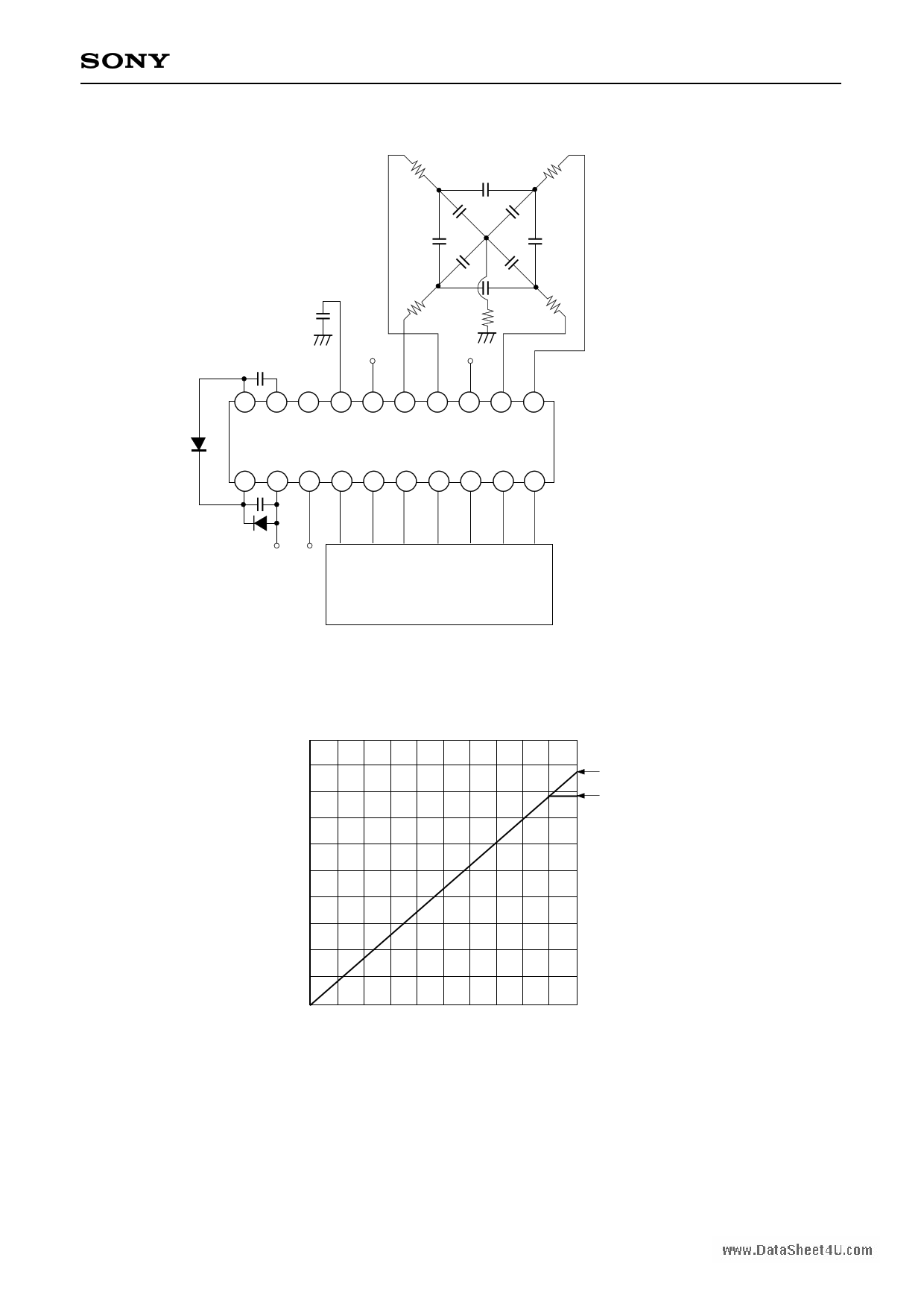
Measurement Circuit
0.1µF
R1 C1
500pF
C2
C1
C2
C2
C2
R1 C1
R2
–8.5V
0V
R1
C1
R1
20 19 18 17 16 15 14 13 12 11
CXD1267AN
1 2 3 4 5 6 7 8 9 10
0.1µF
15V 4.5V
Timing generator (CXD1156Q)
R1; 27Ω
R2; 5Ω
C1; 1500pF
C2; 3300pF
CXD1267AN
Operational Amplifier Gain Characteristics
[V] Ta = –20 to +75°C IDCOUT = 0µA
25.0
At VH = 15V, VL = –8.5V
At VH = 14.5V, VL = –6.0V
2.5/div
0
0.5/div
5.0 [V]
Input voltage
Note) Operating amplifier maximum output voltage is restricted as shown in the formula below depending on
supply voltage setting of VH and VL.
Maximum output voltage VDCOUT (max) ≈ VH + | VL | – 0.8V
For instance, when VH = 14.5V and VL = –6.0V, output voltage is saturated at approximately 19.7V as
shown above figure.
–5–
5 Page | ||
| Páginas | Total 8 Páginas | |
| PDF Descargar | [ Datasheet D1267.PDF ] | |
Hoja de datos destacado
| Número de pieza | Descripción | Fabricantes |
| D1260 | METAL GATE RF SILICON FET | Seme LAB |
| D1260UK | METAL GATE RF SILICON FET | Seme LAB |
| D1262 | NPN Transistor - 2SD1262 | Panasonic |
| D1262A | NPN Transistor - 2SD1262A | Panasonic |
| Número de pieza | Descripción | Fabricantes |
| SLA6805M | High Voltage 3 phase Motor Driver IC. |
Sanken |
| SDC1742 | 12- and 14-Bit Hybrid Synchro / Resolver-to-Digital Converters. |
Analog Devices |
|
DataSheet.es es una pagina web que funciona como un repositorio de manuales o hoja de datos de muchos de los productos más populares, |
| DataSheet.es | 2020 | Privacy Policy | Contacto | Buscar |
