|
|
|
PDF AD10200 Data sheet ( Hoja de datos )
| Número de pieza | AD10200 | |
| Descripción | 12-Bit 105 MSPS IF Sampling A/D Converter | |
| Fabricantes | Analog Devices | |
| Logotipo | ||
Hay una vista previa y un enlace de descarga de AD10200 (archivo pdf) en la parte inferior de esta página. Total 20 Páginas | ||
|
No Preview Available !
a
Dual Channel, 12-Bit 105 MSPS IF Sampling
A/D Converter with Analog Input
Signal Conditioning
FEATURES
Dual, 105 MSPS Minimum Sample Rate
Channel-Channel Isolation, >80 dB
AC-Coupled Signal Conditioning Included
Gain Flatness up to Nyquist: < 0.2 dB
Input VSWR 1.1:1 to Nyquist
80 dB Spurious-Free Dynamic Range
Two’s Complement Output Format
3.3 V or 5 V CMOS-Compatible Output Levels
0.850 W per Channel
Industrial and Military Grade
APPLICATIONS
Radar IF Receivers
Phased Array Receivers
Communications Receivers
Secure Communications
GPS Antijamming Receivers
Multichannel, Multimode Receivers
PRODUCT DESCRIPTION
The AD10200 is a full channel ADC solution with on-module
signal conditioning for improved dynamic performance and
fully matched channel-to-channel performance. The module
AD10200
includes two wide-dynamic range ADCs. Each ADC has a
transformer coupled front-end optimized for Direct-IF sampling.
The AD10200 has on-chip track-and-hold circuitry, and utilizes
an innovative architecture to achieve 12-bit, 105 MSPS perfor-
mance. The AD10200 uses innovative high-density circuit
design to achieve exceptional matching and performance while
still maintaining excellent isolation, and providing for significant
board area savings.
The AD10200 operates with 5.0 V supply for the analog-to-
digital conversion. Each channel is completely independent
allowing operation with independent encode and analog inputs.
The AD10200 is packaged in a 68-lead ceramic chip carrier
package. Manufacturing is done on Analog Devices, Inc. MIL-
38534 Qualified Manufacturers Line (QML) and components
are available up to Class-H (–50°C to +125°C).
PRODUCT HIGHLIGHTS
1. Guaranteed sample rate of 105 MSPS.
2. Input signal conditioning with full power bandwidth to
250 MHz.
3. Fully tested/characterized performance at 121 MHz AIN.
4. Optimized for IF sampling.
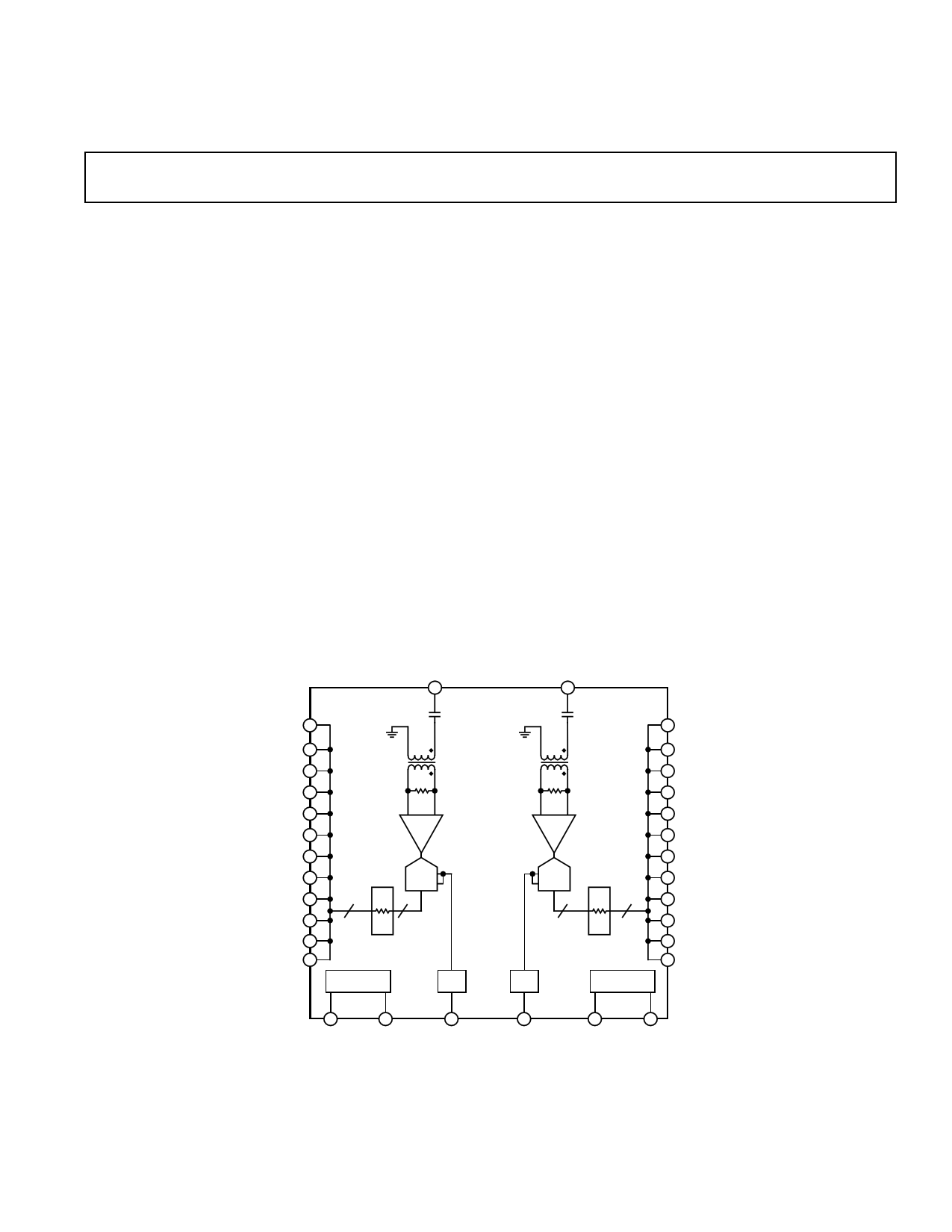
FUNCTIONAL BLOCK DIAGRAM
AINA2
7
AINB2
63
D00A 34
(LSB)
D01A 33
D02A 32
D03A 31
D04A 30
D05A 29
D06A 28
D07A 25
D08A 24
D09A 23
D10A 22
D11A 21
(MSB)
T1A
50⍀
T/H
T1B
AD10200
50⍀
T/H
ADC
12 12
OUTPUT RESISTORS
TIMING
REF
ADC
12
12
OUTPUT RESISTORS
REF
TIMING
50 D00B
(LSB)
49 D01B
48 D02B
47 D03B
46 D04B
45 D05B
42 D06B
41 D07B
40 D08B
39 D09B
38 D10B
37 D11B
(MSB)
18 17
3
ENCODEA ENCODEA REF_A_OUT
56
REF_B_OUT
53 54
ENCODEB ENCODEB
REV. B
Information furnished by Analog Devices is believed to be accurate and
reliable. However, no responsibility is assumed by Analog Devices for its
use, nor for any infringements of patents or other rights of third parties that
may result from its use. No license is granted by implication or otherwise
under any patent or patent rights of Analog Devices.
One Technology Way, P.O. Box 9106, Norwood, MA 02062-9106, U.S.A.
Tel: 781/329-4700
Fax: 781/326-8703
www.analog.com
©Analog Devices, Inc., 2001–2016
1 page 
AD10200
ABSOLUTE MAXIMUM RATINGS1, 2
VDD . . . . . . . . . . . . . . . . . . . . . . . . . . . . . . . . . . . . . . . . . 6 V
VCC . . . . . . . . . . . . . . . . . . . . . . . . . . . . . . . . . . . . . . . . . 6 V
Analog Inputs . . . . . . . . . . . . . . . . . . . . . . . . 5 Vp-p(18 dBm)
Digital Inputs . . . . . . . . . . . . . . . . . . . –0.5 V to VDD + 0.5 V
Digital Output Current . . . . . . . . . . . . . . . . . . . . . . . . 20 mA
Operating Temperature . . . . . . . . . . . . . . . . –50°C to +125°C
Storage Temperature . . . . . . . . . . . . . . . . . . –65°C to +150°C
Maximum Junction Temperature . . . . . . . . . . . . . . . . . 175°C
Maximum Case Temperature . . . . . . . . . . . . . . . . . . . . 150°C
NOTES
1Stresses above those listed under Absolute Maximum Ratings may cause perma-
nent damage to the device. This is a stress rating only; functional operation of the
device at these or any other conditions outside of those indicated in the operation
sections of this specification is not implied. Exposure to absolute maximum ratings
for extended periods may affect device reliability.
2Typical thermal impedances for “Z” package:
θJC = 2.22°C/W; θJA = 24.3°C/W.
EXPLANATION OF TEST LEVELS
Test Level
I. 100% production tested.
II. 100% production tested at 25°C and sample tested at
specific temperatures.
III. Sample tested only.
IV. Parameter is guaranteed by design and characterization
testing.
V. Parameter is a typical value only.
VI. 100% production tested at 25°C; guaranteed by design and
characterization testing for industrial temperature range.
Table I. Output Coding (VREF = 2.5 V) (Two’s Complement)
Code
+2047
•
•
0
–1
•
•
–2048
AIN (V)
+1.024
•
•
0
–0.00049
•
•
–1.024
Digital Output
0111 1111 1111
•
•
0000 0000 0000
1111 1111 1111
•
•
1000 0000 0000
CAUTION
ESD (electrostatic discharge) sensitive device. Electrostatic charges as high as 4000 V readily
accumulate on the human body and test equipment and can discharge without detection. Although
the AD10200 features proprietary ESD protection circuitry, permanent damage may occur on
devices subjected to high-energy electrostatic discharges. Therefore, proper ESD precautions are
recommended to avoid performance degradation or loss of functionality.
WARNING!
ESD SENSITIVE DEVICE
Revision History
Location
Page
8/2016 Data Sheet changed from REV. A to REV. B.
Change Operating Temperature Range. . . . . . . . . . . . . . . . . . . . . . . . . . . . . . . . . . . . . . . . . . . . . . . . . . . . . . . . . . . . . . . . . . . . . .1, 4
Moved Ordering Guide . . . . . . . . . . . . . . . . . . . . . . . . . . . . . . . . . . . . . . . . . . . . . . . . . . . . . . . . . . . . . . . . . . . . . . . . . . . . . . . . . . . . 19
Changes to Ordering Guide . . . . . . . . . . . . . . . . . . . . . . . . . . . . . . . . . . . . . . . . . . . . . . . . . . . . . . . . . . . . . . . . . . . . . . . . . . . . . . 19
Updated Outline Dimensions . . . . . . . . . . . . . . . . . . . . . . . . . . . . . . . . . . . . . . . . . . . . . . . . . . . . . . . . . . . . . . . . . . . . . . . . . . . . 19
Data Sheet changed from REV. 0 to REV. A.
Edit to ABSOLUTE MAXIMUM RATINGS . . . . . . . . . . . . . . . . . . . . . . . . . . . . . . . . . . . . . . . . . . . . . . . . . . . . . . . . . . . . . . . . . 4
Edit to Figure 5 . . . . . . . . . . . . . . . . . . . . . . . . . . . . . . . . . . . . . . . . . . . . . . . . . . . . . . . . . . . . . . . . . . . . . . . . . . . . . . . . . . . . . . . . . 9
Edit to ENCODE Inputs section . . . . . . . . . . . . . . . . . . . . . . . . . . . . . . . . . . . . . . . . . . . . . . . . . . . . . . . . . . . . . . . . . . . . . . . . . . . 10
Edit to Figure 9a . . . . . . . . . . . . . . . . . . . . . . . . . . . . . . . . . . . . . . . . . . . . . . . . . . . . . . . . . . . . . . . . . . . . . . . . . . . . . . . . . . . . . . . 12
–4– REV. B
5 Page 
AD10200
APPLICATION NOTES
Theory of Operation
The AD10200 is a high-dynamic range dual 12-bit, 105 MHz
subrange pipeline converter that uses switched capacitor
architecture. The analog input section uses AINA2/AINB2 at
2.048 V p-p with an input impedance of 50 Ω. The analog input
includes an ac-coupled wide-band 1:1 transformer, which provides
high-dynamic range and SNR while maintaining VSWR and
gain flatness. The ADC includes a high-bandwidth linear track/
hold that gives excellent spurious performance up to and beyond
the Nyquist rate. The high-bandwidth track/hold has a low jitter
of 0.25 ps rms, leading to excellent SNR and SFDR performance.
AC-coupled differential PECL/ECL encode inputs are recom-
mended for optimum performance.
USING THE AD10200
ENCODE Input
Any high speed A/D converter is extremely sensitive to the quality
of the sampling clock provided by the user. A track/hold circuit
is essentially a mixer, and any noise, distortion, or timing jitter
on the clock will be combined with the desired signal at the A/D
output. For that reason, considerable care has been taken in the
design of the ENCODE input of the AD10200, and the user is
advised to give commensurate thought to the clock source. The
ENCODE input are fully TTL/CMOS compatible. For opti-
mum performance, the AD10200 must be clocked differentially.
Note that the ENCODE inputs cannot be driven directly from
PECL level signals (VIHD is 3.5 V max). PECL level signals can
easily be accommodated by ac coupling as shown in Figure 6.
Good performance is obtained using an MC10EL16 in the
circuit to drive the encode inputs.
PECL
GATE
510⍀
0.1F
510⍀ 0.1F
AD10200
ENCODE
ENCODE
GND
Figure 6. AC Coupling to ENCODE Inputs
ENCODE Voltage Level Definition
The voltage level definitions for driving ENCODE and ENCODE
in differential mode are shown in Figure 7.
ENCODE Inputs
Differential Signal Amplitude (VID)
High Differential Input Voltage (VIHD)
Low Differential Input Voltage (VILD)
Common-Mode Input (VICN)
500 mV min,
750 mV nom
5.0 V max
0 V min
1.25 V min, 1.6 V nom
ENCODE
ENCODE
ENCODE
VIHD
VICM
VILD
VIHS
VID
0.1F
VILS
Figure 7. Differential Input Levels
Often, the cleanest clock source is a crystal oscillator producing
a pure sine wave. In this configuration, or with any roughly
symmetrical clock input, the input can be ac-coupled and biased
to a reference voltage that also provides the ENCODE. This
ensures that the reference voltage is centered on the encode signal.
Digital Outputs
The digital outputs are TTL/CMOS-compatible and a separate
output power supply pin supports interfacing with 3.3 V logic.
Analog Input
The analog input is a single ended ac-coupled high performance
1:1 transformer with an input impedance of 50 Ω to 105 MHz.
The nominal full scale input is 2.048 V p-p.
Special care was taken in the design of the analog input section
of the AD10200 to prevent damage and corruption of data when
the input is overdriven.
Voltage Reference
A stable and accurate 2.5 V voltage reference is designed into
the AD10200 (VREFOUT). An external voltage reference is
not required.
Timing
The AD10200 provides latched data outputs, with 10 pipeline
delays. Data outputs are available one propagation delay (tPD)
after the rising edge of the encode command (see Figure 1). The
length of the output data lines and loads placed on them should
be minimized to reduce transients within the AD10200; these
transients can detract from the converter's dynamic performance.
The minimum guaranteed conversion rate of the AD10200 is
10 MSPS. At internal clock rates below 10 MSPS, dynamic
performance may degrade. Therefore, input clock rates below
10 MHz should be avoided.
GROUNDING AND DECOUPLING
Analog and Digital Grounding
Proper grounding is essential in any high speed, high resolution
system. Multilayer printed circuit boards (PCBs) are recom-
mended to provide optimal grounding and power schemes. The
use of ground and power planes offers distinct advantages:
1. The minimization of the loop area encompassed by a signal
and its return path.
2. The minimization of the impedance associated with ground
and power paths.
3. The inherent distributed capacitor formed by the power
plane, PCB insulation and ground plane.
These characteristics result in both a reduction of electromagnetic
interference (EMI) and an overall improvement in performance.
It is important to design a layout that prevents noise from cou-
pling to the input signal. Digital signals should not be run in
parallel with input signal traces and should be routed away from
the input circuitry. The PCB should have a ground plane covering
all unused portions of the component side of the board to pro-
vide a low impedance path and manage the power and ground
currents. The ground plane should be removed from the area
near the input pins to reduce stray capacitance.
–10–
REV. B
11 Page | ||
| Páginas | Total 20 Páginas | |
| PDF Descargar | [ Datasheet AD10200.PDF ] | |
Hoja de datos destacado
| Número de pieza | Descripción | Fabricantes |
| AD1020 | (AD1xxx) Hybrid IC | Nichicon |
| AD10200 | 12-Bit 105 MSPS IF Sampling A/D Converter | Analog Devices |
| Número de pieza | Descripción | Fabricantes |
| SLA6805M | High Voltage 3 phase Motor Driver IC. |
Sanken |
| SDC1742 | 12- and 14-Bit Hybrid Synchro / Resolver-to-Digital Converters. |
Analog Devices |
|
DataSheet.es es una pagina web que funciona como un repositorio de manuales o hoja de datos de muchos de los productos más populares, |
| DataSheet.es | 2020 | Privacy Policy | Contacto | Buscar |