|
|
|
PDF AD5546 Data sheet ( Hoja de datos )
| Número de pieza | AD5546 | |
| Descripción | 16-/14-Bit Multiplying DAC | |
| Fabricantes | Analog Devices | |
| Logotipo | ||
Hay una vista previa y un enlace de descarga de AD5546 (archivo pdf) en la parte inferior de esta página. Total 20 Páginas | ||
|
No Preview Available !
Data Sheet
Current Output, Parallel Input, 16-/14-Bit
Multiplying DACs with Four-Quadrant Resistors
AD5546/AD5556
FEATURES
16-bit resolution
14-bit resolution
2- or 4-quadrant multiplying DAC
±1 LSB DNL
±1 LSB INL
Operating supply voltage: 2.7 V to 5.5 V
Low noise: 12 nV/√Hz
Low power: IDD = 10 μA
0.5 μs settling time
Built-in RFB facilitates current-to-voltage conversion
Built-in 4-quadrant resistors allow 0 V to –10 V, 0 V to +10 V,
or ±10 V outputs
2 mA full-scale current ±20%, with VREF = 10 V
Automotive operating temperature: –40°C to +125°C
Compact TSSOP-28 package
APPLICATIONS
Automatic test equipment
Instrumentation
Digitally controlled calibration
Digital waveform generation
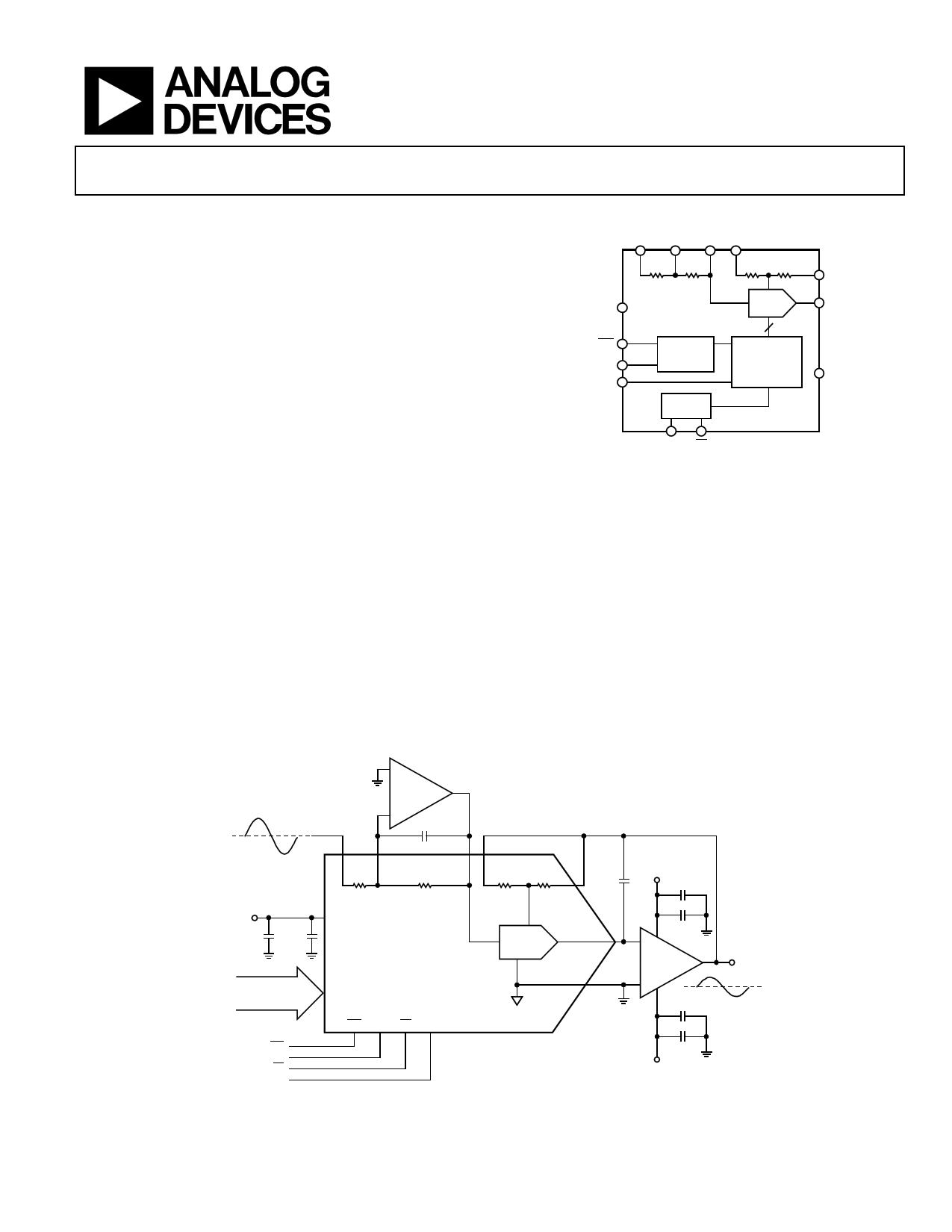
FUNCTIONAL BLOCK DIAGRAM
R1 RCOM REF ROFS
R1 R2
ROFS RFB
RFB
VDD
WR
LDAC
DB0 TO DB15
AD5546/
AD5556
CONTROL
LOGIC
DAC
16/14
DAC
REGISTER
IOUT
GND
POR
MSB RS
Figure 1. AD5546/AD5556 Simplified Block Diagram
GENERAL DESCRIPTION
The AD5546/AD5556 are precision 16-/14-bit, multiplying, low
power, current output, parallel input digital-to-analog converters
(DACs). They operate from a single 2.7 V to 5.5 V supply with
±10 V multiplying references for four-quadrant outputs. Built-
in four-quadrant resistors facilitate the resistance matching and
temperature tracking that minimize the number of components
needed for multiquadrant applications. The feedback resistor
(RFB) simplifies the I-V conversion with an external buffer. The
AD5546/AD5556 are packaged in compact TSSOP-28 packages
with operating temperatures from –40°C to +125°C.
The EVAL-AD5546SDZ is available for evaluating DAC perfor-
mance. For more information, see the UG-309 evaluation board
user guide.
+10V
+
U2A
OP2177
–
C7
–10V
R1A
RCOMA
VREFA
R1 R2
ROFSA RFBA
ROFS
RFB
+15V
C6
C4
1µF
+5V
C1
1µF
C2
0.1µF
16-/14-BIT
DATA
VDD
U1
AD5546/AD5556
16-/14-BIT
DATA
IOUT
GND
C5
– V+ 0.1µF
U2B
OP2177
+ V–
C8
1µF
VOUT
WR LDAC RS MSB
WR
LDAC
RS
MSB
C9
0.1µF
–15V
Figure 2. 16-/14-Bit, Four-Quadrant Multiplying DAC with a Minimum of External Components
Rev. D
Information furnished by Analog Devices is believed to be accurate and reliable. However, no
responsibility is assumed by Analog Devices for its use, nor for any infringements of patents or other
rights of third parties that may result from its use. Specifications subject to change without notice. No
license is granted by implication or otherwise under any patent or patent rights of Analog Devices.
Trademarksandregisteredtrademarksarethepropertyoftheirrespectiveowners.
One Technology Way, P.O. Box 9106, Norwood, MA 02062-9106, U.S.A.
Tel: 781.329.4700
www.analog.com
Fax: 781.461.3113 ©2004-2011 Analog Devices, Inc. All rights reserved.
1 page 
Data Sheet
ABSOLUTE MAXIMUM RATINGS
Table 2.
Parameter
VDD to GND
RFB, ROFS, R1, RCOM, and REF to GND
Logic Inputs to GND
V (IOUT) to GND
Input Current to Any Pin Except Supplies
Thermal Resistance (θJA)
Maximum Junction Temperature (TJ MAX)
Operating Temperature Range
Storage Temperature Range
Lead Temperature:
Vapor Phase, 60 s
Infrared, 15 s
Package Power Dissipation
Rating
–0.3 V, +8 V
–18 V, 18 V
–0.3 V, +8 V
–0.3 V, VDD + 0.3 V
±50 mA
128°C
150°C
–40°C to +125°C
–65°C to +150°C
215°C
220°C
(TJ MAX – TA)/θJA
AD5546/AD5556
Stresses above those listed under Absolute Maximum Ratings
may cause permanent damage to the device. This is a stress
rating only; functional operation of the device at these or any
other conditions above those listed in the operational sections
of this specification is not implied. Exposure to absolute
maximum rating conditions for extended periods may affect
device reliability.
ESD CAUTION
Rev. D | Page 5 of 20
5 Page 
Data Sheet
AD5546/AD5556
DIGITAL SECTION
The AD5546/AD5556 have 16-/14-bit parallel inputs. The devices are double buffered with 16-/14-bit registers. The double-buffered
feature allows the update of several AD5546/AD5556 simultaneously. For the AD5546, the input register is loaded directly from a 16-bit
controller bus when the WR pin is brought low. The DAC register is updated with data from the input register when LDAC is brought
high. Updating the DAC register updates the DAC output with the new data (see Figure 17). To make both registers transparent, tie WR
low and LDAC high. The asynchronous RS pin resets the part to zero scale if the MSB pin = 0 and to midscale if the MSB pin = 1.
Table 5. AD5546 Parallel Input Data Format
MSB
LSB
Bit Position
B15 B14 B13 B12 B11 B10 B9 B8 B7 B6 B5 B4 B3 B2 B1 B0
Data Word
D15 D14 D13 D12 D11 D10 D9 D8 D7 D6 D5 D4 D3 D2 D1 D0
Table 6. AD5556 Parallel Input Data Format
MSB
LSB
Bit Position B13 B12 B11 B10 B9 B8 B7 B6 B5 B4 B3 B2 B1 B0
Data Word
D13 D12 D11 D10 D9 D8 D7 D6 D5 D4 D3 D2 D1 D0
Table 7. Control Inputs
RS WR LDAC Register Operation
0 X1
X1
Reset output to 0, with MSB pin = 0 and to midscale with MSB pin = 1.
10
0
Load input register with data bits.
11
1
Load DAC register with the contents of the input register.
10
1
Input and DAC registers are transparent.
1 When LDAC and WR are tied together and programmed as a pulse, the data bits are loaded into the input register on
the falling edge of the pulse and then loaded into the DAC register on the rising edge of the pulse.
11
0
No register operation.
1 X = don’t care.
ESD PROTECTION CIRCUITS
All logic input pins contain back-biased ESD protection Zeners
connected to ground (GND) and VDD, as shown in Figure 18. As
a result, the voltage level of the logic input should not be greater
than the supply voltage.
VDD
DIGITAL
INPUTS 5kΩ
DGND
Figure 18. Equivalent ESD Protection Circuits
AMPLIFIER SELECTION
In addition to offset voltage, the bias current is important in op
amp selection for precision current output DACs. An input bias
current of 30 nA in the op amp contributes to 1 LSB in the
AD5546’s full-scale error. The OP1177 and AD8628 op amps
are good candidates for the I-V conversion.
REFERENCE SELECTION
The initial accuracy and the rated output of the voltage refer-
ence determine the full span adjustment. The initial accuracy is
usually a secondary concern in precision because it can be
trimmed. Figure 23 shows an example of a trimming circuit.
The zero scale error can also be minimized by standard op amp
nulling techniques.
The voltage reference temperature coefficient (TC) and long-
term drift are primary considerations. For example, a 5 V ref-
erence with a TC of 5 ppm/oC means that the output changes by
25 µV per degree Celsius. As a result, the reference that operates
at 55oC contributes an additional 750 µV full-scale error.
Similarly, the same 5 V reference with a ±50 ppm long-term
drift means that the output may change by ±250 µV over time.
Therefore, it is practical to calibrate a system periodically to
maintain its optimum precision.
Rev. D | Page 11 of 20
11 Page | ||
| Páginas | Total 20 Páginas | |
| PDF Descargar | [ Datasheet AD5546.PDF ] | |
Hoja de datos destacado
| Número de pieza | Descripción | Fabricantes |
| AD5541 | 5 V/ Serial-Input Voltage-Output/ 16-Bit DACs | Analog Devices |
| AD5541A | (AD5512A - AD5542A) 16-/12-Bit NanoDAC | Analog Devices |
| AD5542 | 5 V/ Serial-Input Voltage-Output/ 16-Bit DACs | Analog Devices |
| AD5542A | (AD5512A - AD5542A) 16-/12-Bit NanoDAC | Analog Devices |
| Número de pieza | Descripción | Fabricantes |
| SLA6805M | High Voltage 3 phase Motor Driver IC. |
Sanken |
| SDC1742 | 12- and 14-Bit Hybrid Synchro / Resolver-to-Digital Converters. |
Analog Devices |
|
DataSheet.es es una pagina web que funciona como un repositorio de manuales o hoja de datos de muchos de los productos más populares, |
| DataSheet.es | 2020 | Privacy Policy | Contacto | Buscar |