|
|
|
PDF AD5542 Data sheet ( Hoja de datos )
| Número de pieza | AD5542 | |
| Descripción | 5 V/ Serial-Input Voltage-Output/ 16-Bit DACs | |
| Fabricantes | Analog Devices | |
| Logotipo | ||
Hay una vista previa y un enlace de descarga de AD5542 (archivo pdf) en la parte inferior de esta página. Total 12 Páginas | ||
|
No Preview Available !
a
5 V, Serial-Input
Voltage-Output, 16-Bit DACs
AD5541/AD5542
FEATURES
Full 16-Bit Performance
5 V Single Supply Operation
Low Power
Short Settling Time
Unbuffered Voltage Output Capable of Driving 60 k⍀
Loads Directly
SPI™/QSPI™/MICROWIRE™-Compatible Interface
Standards
Power-On Reset Clears DAC Output to 0 V (Unipolar
Mode)
Schmitt Trigger Inputs for Direct Optocoupler Interface
APPLICATIONS
Digital Gain and Offset Adjustment
Automatic Test Equipment
Data Acquisition Systems
Industrial Process Control
GENERAL DESCRIPTION
The AD5541 and AD5542 are single, 16-bit, serial input,
voltage output DACs that operate from a single 5 V ± 10%
supply.
The AD5541 and AD5542 utilize a versatile 3-wire interface that
is compatible with SPI, QSPI, MICROWIRE, and DSP inter-
face standards.
These DACs provide 16-bit performance without any adjust-
ments. The DAC output is unbuffered, which reduces power
consumption and offset errors contributed to by an output buffer.
The AD5542 can be operated in bipolar mode generating a
± VREF output swing. The AD5542 also includes Kelvin sense
connections for the reference and analog ground pins to reduce
layout sensitivity.
The AD5541 and AD5542 are available in an SO package.
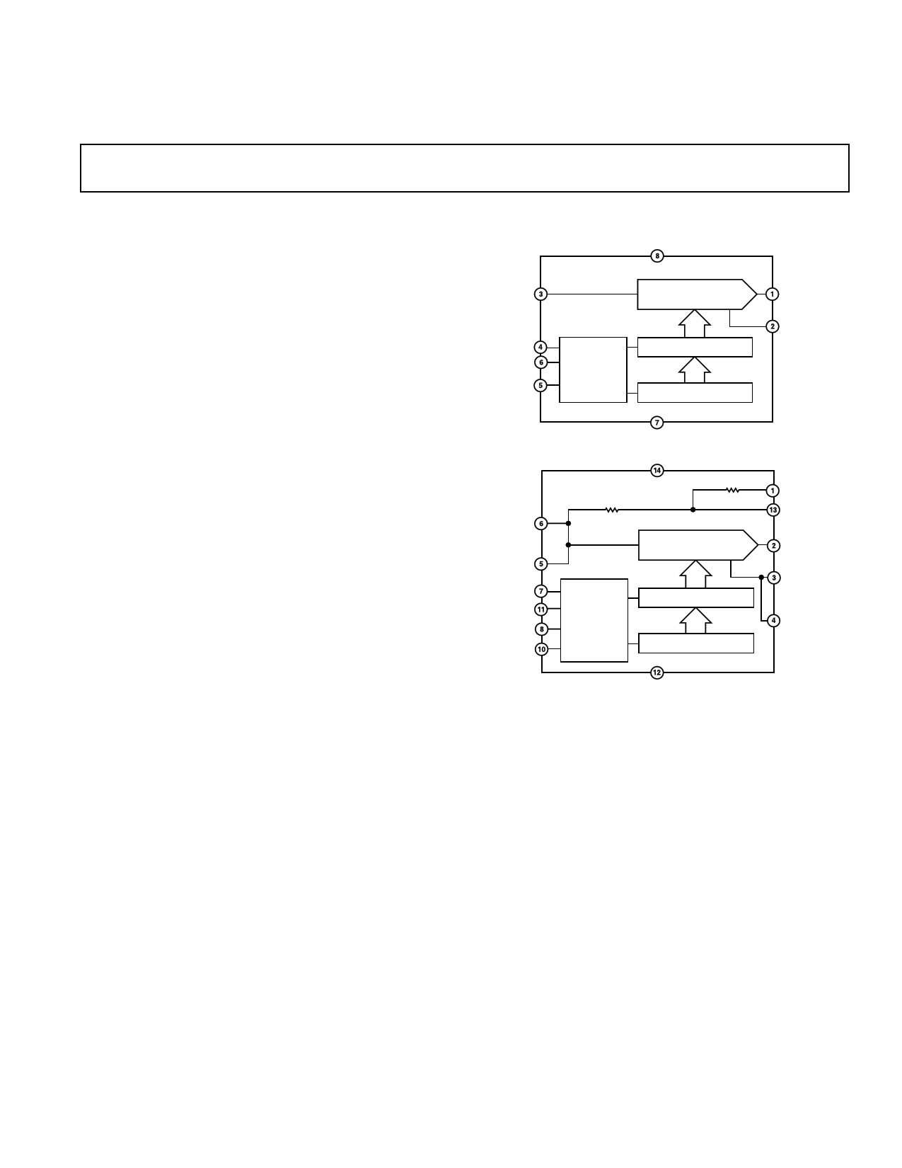
FUNCTIONAL BLOCK DIAGRAMS
AD5541
REF
VDD
16-BIT DAC
VOUT
CS
DIN
SCLK
CONTROL
LOGIC
16-BIT DATA LATCH
SERIAL INPUT REGISTER
AGND
REFF
REFS
CS
LDAC
SCLK
DIN
AD5542
RINV
CONTROL
LOGIC
DGND
VDD
RFB
16-BIT DAC
16-BIT DATA LATCH
SERIAL INPUT REGISTER
DGND
RFB
INV
VOUT
AGNDF
AGNDS
PRODUCT HIGHLIGHTS
1. Single Supply Operation.
The AD5541 and AD5542 are fully specified and guaranteed
for a single 5 V ± 10% supply.
2. Low Power Consumption.
These parts consume typically 1.5 mW with a 5 V supply.
3. 3-Wire Serial Interface.
4. Unbuffered output capable of driving 60 kΩ loads.
This reduces power consumption as there is no internal buffer
to drive.
5. Power-On Reset circuitry.
SPI and QSPI are trademarks of Motorola, Inc.
MICROWIRE is a trademark of National Semiconductor Corporation.
REV. A
Information furnished by Analog Devices is believed to be accurate and
reliable. However, no responsibility is assumed by Analog Devices for its
use, nor for any infringements of patents or other rights of third parties
which may result from its use. No license is granted by implication or
otherwise under any patent or patent rights of Analog Devices.
One Technology Way, P.O. Box 9106, Norwood, MA 02062-9106, U.S.A.
Tel: 781/329-4700 World Wide Web Site: http://www.analog.com
Fax: 781/326-8703
© Analog Devices, Inc., 1999
1 page 
Mnemonic
VOUT
AGND
REF
CS
SCLK
DIN
DGND
VDD
Pin No.
1
2
3
4
5
6
7
8
AD5541/AD5542
AD5541 PIN FUNCTION DESCRIPTIONS
Description
Analog Output Voltage from the DAC.
Ground Reference Point for Analog Circuitry.
This is the voltage reference input for the DAC. Connect to external 2.5 V reference.
Reference can range from 2 V to VDD.
This is a logic input signal. The chip select signal is used to frame the serial data input.
Clock Input. Data is clocked into the input register on the rising edge of SCLK. Duty cycle
must be between 40% and 60%.
Serial Data Input. This device accepts 16-bit words. Data is clocked into the input register on
the rising edge of SCLK.
Digital Ground. Ground reference for digital circuitry.
Analog Supply Voltage, 5 V ± 10%.
AD5541 PIN CONFIGURATION
SOIC
AD5542 PIN CONFIGURATION
SOIC
VOUT 1
8 VDD
AGND 2 AD5541 7 DGND
TOP VIEW
REF 3 (Not to Scale) 6 DIN
CS 4
5 SCLK
RFB 1
14 VDD
VOUT 2
13 INV
AGNDF
AGNDS
REFS
3 12 DGND
AD5542
4 TOP VIEW 11 LDAC
5 (Not to Scale) 10 DIN
REFF 6
CS 7
9 NC
8 SCLK
NC = NO CONNECT
Mnemonic
RFB
VOUT
AGNDF
AGNDS
REFS
REFF
CS
SCLK
NC
DIN
LDAC
DGND
INV
VDD
Pin No.
1
2
3
4
5
6
7
8
9
10
11
12
13
14
AD5542 PIN FUNCTION DESCRIPTIONS
Description
Feedback Resistor. In bipolar mode connect this pin to external op amp output.
Analog Output Voltage from the DAC.
Ground Reference Point for Analog Circuitry (Force).
Ground Reference Point for Analog Circuitry (Sense).
This is the voltage reference input (sense) for the DAC. Connect to external 2.5 V reference.
Reference can range from 2 V to VDD.
This is the voltage reference input (force) for the DAC. Connect to external 2.5 V reference.
Reference can range from 2 V to VDD.
This is a logic input signal. The chip select signal is used to frame the serial data input.
Clock input. Data is clocked into the input register on the rising edge of SCLK. Duty cycle
must be between 40% and 60%.
No Connect.
Serial Data Input. This device accepts 16-bit words. Data is clocked into the input register on
the rising edge of SCLK.
LDAC Input. When this input is taken low, the DAC register is simultaneously updated with
the contents of the input register.
Digital Ground. Ground reference for digital circuitry.
Connected to the Internal Scaling Resistors of the DAC. Connect INV pin to external op amps
inverting input in bipolar mode.
Analog Supply Voltage, 5 V ± 10%.
REV. A
–5–
5 Page 
AD5541/AD5542
Reference and Ground
As the input impedance is code-dependent, the reference pin
should be driven from a low-impedance source. The AD5541/
AD5542 operates with a voltage reference ranging from 2 V to
VDD. References below 2 V will result in reduced accuracy.
The DAC’s full-scale output voltage is determined by the
reference. Tables I and II outline the analog output voltage
or particular digital codes. For optimum performance, Kelvin
sense connections are provided on the AD5542.
If the application doesn’t require separate force and sense lines,
they should be tied together close to the package to minimize
voltage drops between the package leads and the internal die.
Power-On Reset
These parts have a power-on reset function to ensure the output
is at a known state upon power-up. On power-up, the DAC
register contains all zeros, until data is loaded from the serial
register. However, the serial register is not cleared on power-up,
so its contents are undefined. When loading data initially to the
DAC, 16 bits or more should be loaded to prevent erroneous
data appearing on the output. If more than 16 bits are loaded,
the last 16 are kept, and if less than 16 are loaded, bits will remain
from the previous word. If the AD5541/AD5542 needs to be
interfaced with data shorter than 16 bits, the data should be
padded with zeros at the LSBs.
Power Supply and Reference Bypassing
For accurate high-resolution performance, it is recommended that
the reference and supply pins be bypassed with a 10 µF tantalum
capacitor in parallel with a 0.1 µF ceramic capacitor.
AD5541/AD5542 to 68HC11 Interface
Figure 22 shows a serial interface between the AD5541/AD5542
and the 68HC11 microcontroller. SCK of the 68HC11 drives
the SCLK of the DAC, while the MOSI output drives the
serial data lines SDIN. CS signal is driven from one of the
port lines. The 68HC11 is configured for master mode; MSTR
= 1, CPOL = 0, and CPHA = 0. Data appearing on the MOSI
output is valid on the rising edge of SCK.
68HC11/
68L11*
PC6
PC7
MOSI
SCK
LDAC**
CS AD5541/
AD5542*
DIN
SCLK
*ADDITIONAL PINS OMITTED FOR CLARITY.
**AD5542 ONLY
Figure 22. AD5541/AD5542 to 68HC11/68L11 Interface
AD5541/AD5542 to MICROWIRE Interface
Figure 23 shows an interface between the AD5541/AD5542 and
any MICROWIRE-compatible device. Serial data is shifted out
on the falling edge of the serial clock and into the AD5541/
AD5542 on the rising edge of the serial clock. No glue logic is
required as the DAC clocks data into the input shift register on
the rising edge.
CS
MICROWIRE* SO
SCLK
CS
DIN AD5541/
AD5542*
SCLK
MICROPROCESSOR INTERFACING
Microprocessor interfacing to the AD5541/AD5542 is via a
serial bus that uses standard protocol compatible with DSP
processors and microcontrollers. The communications channel
requires a 3-wire interface consisting of a clock signal, a data
signal and a synchronization signal. The AD5541/AD5542
requires a 16-bit data word with data valid on the rising edge of
SCLK. The DAC update may be done automatically when all
the data is clocked in or it may be done under control of LDAC
(AD5542 only).
AD5541/AD5542–ADSP-2101/ADSP-2103 Interface
Figure 21 shows a serial interface between the AD5541/AD5542
and the ADSP-2101/ADSP-2103. The ADSP-2101/ADSP-2103
should be set to operate in the SPORT transmit alternate framing
mode. The ADSP-2101/ADSP-2103 is programmed through the
SPORT control register and should be configured as follows:
Internal Clock Operation, Active Low Framing, 16-Bit Word
Length. Transmission is initiated by writing a word to the Tx regis-
ter after the SPORT has been enabled. As the data is clocked out
on each rising edge of the serial clock, an inverter is required
between the DSP and the DAC, because the AD5541/AD5542
clocks data in on the falling edge of the SCLK.
*ADDITIONAL PINS OMITTED FOR CLARITY.
Figure 23. AD5541/AD5542 to MICROWIRE Interface
AD5541/AD5542 to 80C51/80L51 Interface
A serial interface between the AD5541/AD5542 and the 80C51/
80L51 microcontroller is shown in Figure 24. TxD of the
microcontroller drives the SCLK of the AD5541/AD5542, while
RxD drives the serial data line of the DAC. P3.3 is a bit program-
mable pin on the serial port which is used to drive CS.
The 80C51/80L51 provides the LSB first, while the AD5541/
AD5542 expects the MSB of the 16-bit word first. Care should
be taken to ensure the transmit routine takes this into account.
When data is to be transmitted to the DAC, P3.3 is taken low.
Data on RxD is valid on the falling edge of TxD, so the clock must
be inverted as the DAC clocks data into the input shift regis-
ter on the rising edge of the serial clock. The 80C51/80L51
transmits its data in 8-bit bytes with only eight falling clock
edges occurring in the transmit cycle. As the DAC requires a
16-bit word, P3.3 must be left low after the first eight bits are
transferred, and brought high after the second byte is trans-
ferred. LDAC on the AD5542 may also be controlled by
the 80C51/80L51 serial port output by using another bit
programmable pin, P3.4.
FO
ADSP-2101/ TFS
ADSP-2103*
DT
SCLK
LDAC**
CS AD5541/
AD5542*
DIN
SCLK
*ADDITIONAL PINS OMITTED FOR CLARITY.
**AD5542 ONLY
Figure 21. AD5541/AD5542 to ADSP-2101/ADSP-2103
Interface
80C51/
80L51*
P3.4
P3.3
RxD
TxD
LDAC**
CS AD5541/
AD5542*
DIN
SCLK
*ADDITIONAL PINS OMITTED FOR CLARITY.
**AD5542 ONLY
Figure 24. AD5541/AD5542 to 80C51/80L51 Interface
REV. A
–11–
11 Page | ||
| Páginas | Total 12 Páginas | |
| PDF Descargar | [ Datasheet AD5542.PDF ] | |
Hoja de datos destacado
| Número de pieza | Descripción | Fabricantes |
| AD5541 | 5 V/ Serial-Input Voltage-Output/ 16-Bit DACs | Analog Devices |
| AD5541A | (AD5512A - AD5542A) 16-/12-Bit NanoDAC | Analog Devices |
| AD5542 | 5 V/ Serial-Input Voltage-Output/ 16-Bit DACs | Analog Devices |
| AD5542A | (AD5512A - AD5542A) 16-/12-Bit NanoDAC | Analog Devices |
| Número de pieza | Descripción | Fabricantes |
| SLA6805M | High Voltage 3 phase Motor Driver IC. |
Sanken |
| SDC1742 | 12- and 14-Bit Hybrid Synchro / Resolver-to-Digital Converters. |
Analog Devices |
|
DataSheet.es es una pagina web que funciona como un repositorio de manuales o hoja de datos de muchos de los productos más populares, |
| DataSheet.es | 2020 | Privacy Policy | Contacto | Buscar |