|
|
|
PDF AD5161 Data sheet ( Hoja de datos )
| Número de pieza | AD5161 | |
| Descripción | 256-Position SPI/I2C Selectable Digital Potentiometer | |
| Fabricantes | Analog Devices | |
| Logotipo | ||
Hay una vista previa y un enlace de descarga de AD5161 (archivo pdf) en la parte inferior de esta página. Total 20 Páginas | ||
|
No Preview Available !
Data Sheet
FEATURES
256-position
End-to-end resistance 5 kΩ, 10 kΩ, 50 kΩ, 100 kΩ
Compact MSOP-10 (3 mm × 4.9 mm) package
Pin selectable SPI/I2C compatible interface
Extra package address decode pin AD0
Full read/write of wiper register
Power-on preset to midscale
Single supply 2.7 V to 5.5 V
Low temperature coefficient 45 ppm/°C
Low power, IDD = 8 µA
Wide operating temperature −40°C to +125°C
SDO output allows multiple device daisy-chaining
Evaluation board available
APPLICATIONS
Mechanical potentiometer replacement in new designs
Transducer adjustment of pressure, temperature, position,
chemical, and optical sensors
RF amplifier biasing
Gain control and offset adjustment
GENERAL DESCRIPTION
The AD5161 provides a compact 3 mm × 4.9 mm packaged
solution for 256-position adjustment applications. These
devices perform the same electronic adjustment function as
mechanical potentiometers or variable resistors, with enhanced
resolution, solid-state reliability, and superior low temperature
coefficient performance.
The wiper settings are controllable through a pin selectable SPI
or I2C compatible digital interface, which can also be used to
read back the wiper register content. When the SPI mode is
used, the device can be daisy-chained (SDO to SDI), allowing
several parts to share the same control lines. In the I2C mode,
address pin AD0 can be used to place up to two devices on the
same bus. In this same mode, command bits are available to
reset the wiper position to midscale or to shut down the device
into a state of zero power consumption.
Operating from a 2.7 V to 5.5 V power supply and consuming
less than 5 µA allows for usage in portable battery-operated
applications.
256-Position SPI/I2C Selectable
Digital Potentiometer
AD5161
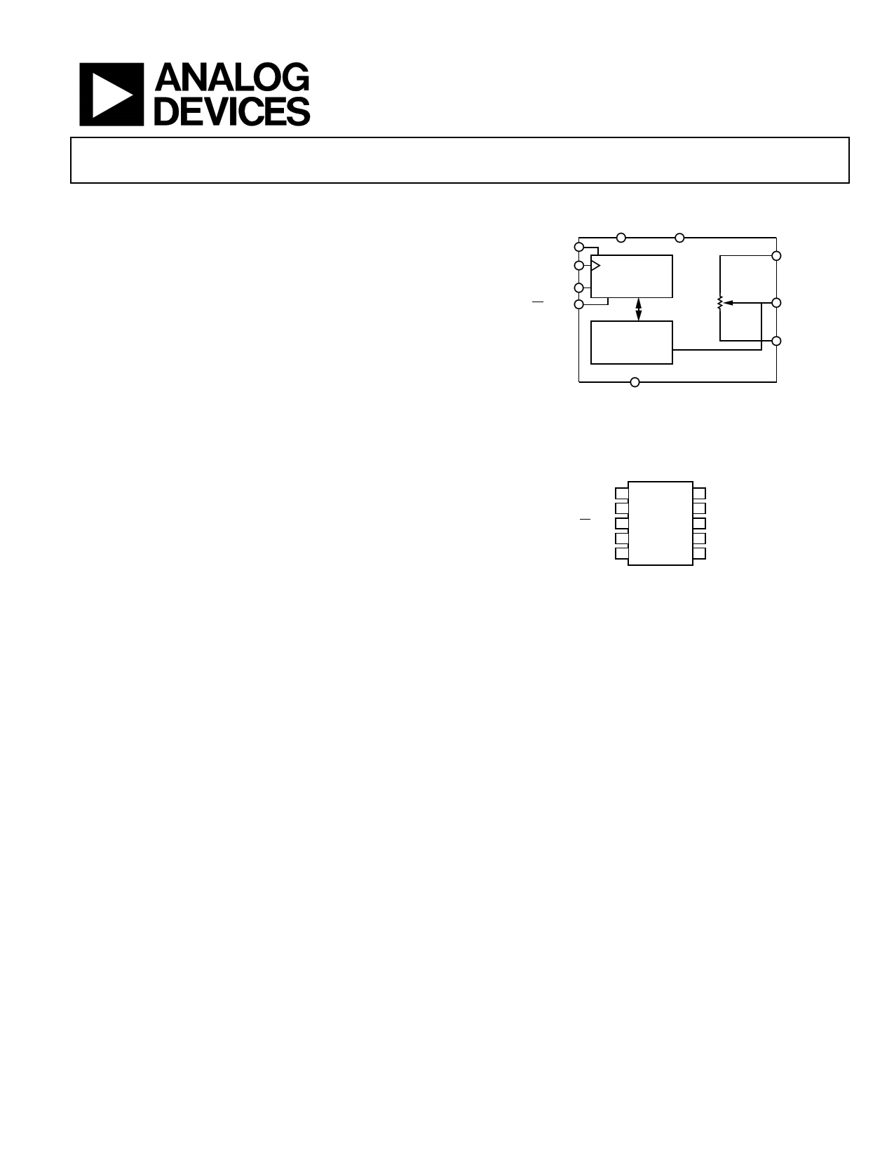
FUNCTIONAL BLOCK DIAGRAM
VDD SDO/NC
SDI/SDA
CLK/SCL
DIS
CS/AD0
SPI OR I2C
INTERFACE
A
W
WIPER
REGISTER
B
GND
Figure 1.
PIN CONFIGURATION
A1
10 W
B 2 AD5161 9 VDD
CS/ADO 3 TOP VIEW 8 DIS
SDO/NC 4 (Not to Scale) 7 GND
SDI/SDA 5
6 CLK/SCL
Figure 2.
Rev. B
Information furnished by Analog Devices is believed to be accurate and reliable. However, no
responsibilityisassumedbyAnalogDevices for itsuse,nor foranyinfringementsofpatentsor other
rights of third parties that may result from its use. Specifications subject to change without notice. No
license is granted by implication or otherwise under any patent or patent rights of Analog Devices.
Trademarksandregisteredtrademarksarethepropertyoftheirrespectiveowners.
One Technology Way, P.O. Box 9106, Norwood, MA 02062-9106, U.S.A.
Tel: 781.329.4700
www.analog.com
Fax: 781.461.3113 ©2003–2012 Analog Devices, Inc. All rights reserved.
1 page 
Data Sheet
AD5161
TIMING CHARACTERISTICS—5 kΩ, 10 kΩ, 50 kΩ, 100 kΩ VERSIONS
VDD = +5V ± 10%, or +3V ± 10%; VA = VDD; VB = 0 V; –40°C < TA < +125°C; unless otherwise noted.
Table 3.
Parameter
Symbol Conditions
SPI INTERFACE TIMING CHARACTERISTICS6, 10 (Specifications Apply to All Parts)
Clock Frequency
Input Clock Pulsewidth
Data Setup Time
Data Hold Time
CS Setup Time
CS High Pulsewidth
fCLK
tCH, tCL
tDS
tDH
tCSS
tCSW
Clock level high or low
CLK Fall to CS Fall Hold Time
tCSH0
CLK Fall to CS Rise Hold Time
tCSH1
CS Rise to Clock Rise Setup
tCS1
I2C INTERFACE TIMING CHARACTERISTICS6, 11 (Specifications Apply to All Parts)
SCL Clock Frequency
tBUF Bus Free Time between STOP and START
tHD;STA Hold Time (Repeated START)
fSCL
t1
t2
After this period, the first clock pulse is
generated.
tLOW Low Period of SCL Clock
tHIGH High Period of SCL Clock
tSU;STA Setup Time for Repeated START Condition
tHD;DAT Data Hold Time
tSU;DAT Data Setup Time
tF Fall Time of Both SDA and SCL Signals
tR Rise Time of Both SDA and SCL Signals
tSU;STO Setup Time for STOP Condition
t3
t4
t5
t6
t7
t8
t9
t10
Min Typ1 Max
25
20
5
5
15
40
0
0
10
400
1.3
0.6
1.3
0.6 50
0.6
0.9
100
300
300
0.6
NOTES
1 Typical specifications represent average readings at +25°C and VDD = 5 V.
2 Resistor position nonlinearity error R-INL is the deviation from an ideal value measured between the maximum resistance and the minimum resistance wiper
positions. R-DNL measures the relative step change from ideal between successive tap positions. Parts are guaranteed monotonic.
3 VAB = VDD, Wiper (VW) = no connect.
4 INL and DNL are measured at VW with the RDAC configured as a potentiometer divider similar to a voltage output D/A converter. VA = VDD and VB = 0 V.
DNL specification limits of ±1 LSB maximum are guaranteed monotonic operating conditions.
5 Resistor terminals A, B, W have no limitations on polarity with respect to each other.
6 Guaranteed by design and not subject to production test.
7 Measured at the A terminal. The A terminal is open circuited in shutdown mode.
8 PDISS is calculated from (IDD × VDD). CMOS logic level inputs result in minimum power dissipation.
9 All dynamic characteristics use VDD = 5 V.
10 See timing diagram for location of measured values. All input control voltages are specified with tR = tF = 2 ns (10% to 90% of 3 V) and timed from a voltage
level of 1.5 V.
11 See timing diagrams for locations of measured values.
Unit
MHz
ns
ns
ns
ns
ns
ns
ns
ns
kHz
µs
µs
µs
µs
µs
µs
ns
ns
ns
µs
Rev. B | Page 5 of 20
5 Page 
Data Sheet
REF LEVEL
–5.000dB
–5.5
/DIV
0.500dB
–6.0
–6.5
–7.0
–7.5
–8.0
–8.5
–9.0
–9.5
R = 100kΩ
R = 50kΩ
R = 10kΩ
–10.0
–10.5
10k
100k
START 1 000.000Hz
5kΩ – 1.026 MHz
10kΩ – 511 MHz
50kΩ – 101 MHz
100kΩ – 54 MHz
R = 5kΩ
1M 10M
STOP 1 000 000.000Hz
Figure 22. –3 dB Bandwidth @ Code = 0x80
60
CODE = 0x80, VA= VDD, VB = 0V
40
PSRR @ VDD = 3V DC ± 10% p-p AC
20
PSRR @ VDD = 5V DC ± 10% p-p AC
0
100
1k 10k
FREQUENCY (Hz)
100k
Figure 23. PSRR vs. Frequency
900
VDD = 5V
800
700
600
500
400
300
200
100
0
10k
CODE = 0x55
CODE = 0xFF
100k
1M
FREQUENCY (Hz)
Figure 24. IDD vs. Frequency
1M
10M
AD5161
1 VW
CLK
2
Ch 1 200mV BW Ch 2 5.00 V BW M 100ns A CH2 3.00 V
Figure 25. Digital Feedthrough
VA = 5V
VB = 0V
1 VW
CS
2
Ch 1 100mV BW Ch 2 5.00 V BW M 200ns A CH1 152mV
Figure 26. Midscale Glitch, Code 0x80–0x7F
VA = 5V
VB = 0V
1 VW
CS
2
Ch 1 5.00V BW Ch 2 5.00 V BW M 200ns A CH1 3.00 V
Figure 27. Large Signal Settling Time, Code 0xFF–0x00
Rev. B | Page 11 of 20
11 Page | ||
| Páginas | Total 20 Páginas | |
| PDF Descargar | [ Datasheet AD5161.PDF ] | |
Hoja de datos destacado
| Número de pieza | Descripción | Fabricantes |
| AD516 | (AD513 / AD516) HIGH SPEED FET-INPUT OP AMPS | ETC |
| AD5160 | 256-Position SPI-Compatible Digital Potentiometer | Analog Devices |
| AD5161 | 256-Position SPI/I2C Selectable Digital Potentiometer | Analog Devices |
| AD5162 | SPI Digital Potentiometer | Analog Devices |
| Número de pieza | Descripción | Fabricantes |
| SLA6805M | High Voltage 3 phase Motor Driver IC. |
Sanken |
| SDC1742 | 12- and 14-Bit Hybrid Synchro / Resolver-to-Digital Converters. |
Analog Devices |
|
DataSheet.es es una pagina web que funciona como un repositorio de manuales o hoja de datos de muchos de los productos más populares, |
| DataSheet.es | 2020 | Privacy Policy | Contacto | Buscar |