|
|
|
PDF AD9762 Data sheet ( Hoja de datos )
| Número de pieza | AD9762 | |
| Descripción | 12-Bit/ 125 MSPS TxDAC D/A Converter | |
| Fabricantes | Analog Devices | |
| Logotipo | ||
Hay una vista previa y un enlace de descarga de AD9762 (archivo pdf) en la parte inferior de esta página. Total 23 Páginas | ||
|
No Preview Available !
a
12-Bit, 125 MSPS
TxDAC® D/A Converter
AD9762*
FEATURES
Member of Pin-Compatible TxDAC Product Family
125 MSPS Update Rate
12-Bit Resolution
Excellent Spurious Free Dynamic Range Performance
SFDR to Nyquist @ 5 MHz Output: 70 dBc
Differential Current Outputs: 2 mA to 20 mA
Power Dissipation: 175 mW @ 5 V to 45 mW @ 3 V
Power-Down Mode: 25 mW @ 5 V
On-Chip 1.20 V Reference
Single +5 V or +3 V Supply Operation
Package: 28-Lead SOIC and TSSOP
Edge-Triggered Latches
APPLICATIONS
Communication Transmit Channel:
Basestations (Single/Multichannel Applications)
ADSL/HFC Modems
Direct Digital Synthesis (DDS)
Instrumentation
PRODUCT DESCRIPTION
The AD9762 is the 12-bit resolution member of the TxDAC
series of high performance, low power CMOS digital-to-analog
converters (DACs). The TxDAC family which consists of pin
compatible 8-, 10-, 12-, and 14-bit DACs is specifically opti-
mized for the transmit signal path of communication systems.
All of the devices share the same interface options, small outline
package and pinout, thus providing an upward or downward
component selection path based on performance, resolution and
cost. The AD9762 offers exceptional ac and dc performance
while supporting update rates up to 125 MSPS.
The AD9762’s flexible single-supply operating range of 2.7 V to
5.5 V and low power dissipation are well suited for portable and
low power applications. Its power dissipation can be further
reduced to a mere 45 mW without a significant degradation in
performance by lowering the full-scale current output. Also, a
power-down mode reduces the standby power dissipation to
approximately 25 mW.
The AD9762 is manufactured on an advanced CMOS process.
A segmented current source architecture is combined with a
proprietary switching technique to reduce spurious components
and enhance dynamic performance. Edge-triggered input
latches and a 1.2 V temperature compensated bandgap refer-
ence have been integrated to provide a complete monolithic
DAC solution. Flexible supply options support +3 V and +5 V
CMOS logic families.
The AD9762 is a current-output DAC with a nominal full-scale
output current of 20 mA and > 100 kΩ output impedance.
TxDAC is a registered trademark of Analog Devices, Inc.
*Patent pending.
REV. B
Information furnished by Analog Devices is believed to be accurate and
reliable. However, no responsibility is assumed by Analog Devices for its
use, nor for any infringements of patents or other rights of third parties
which may result from its use. No license is granted by implication or
otherwise under any patent or patent rights of Analog Devices.
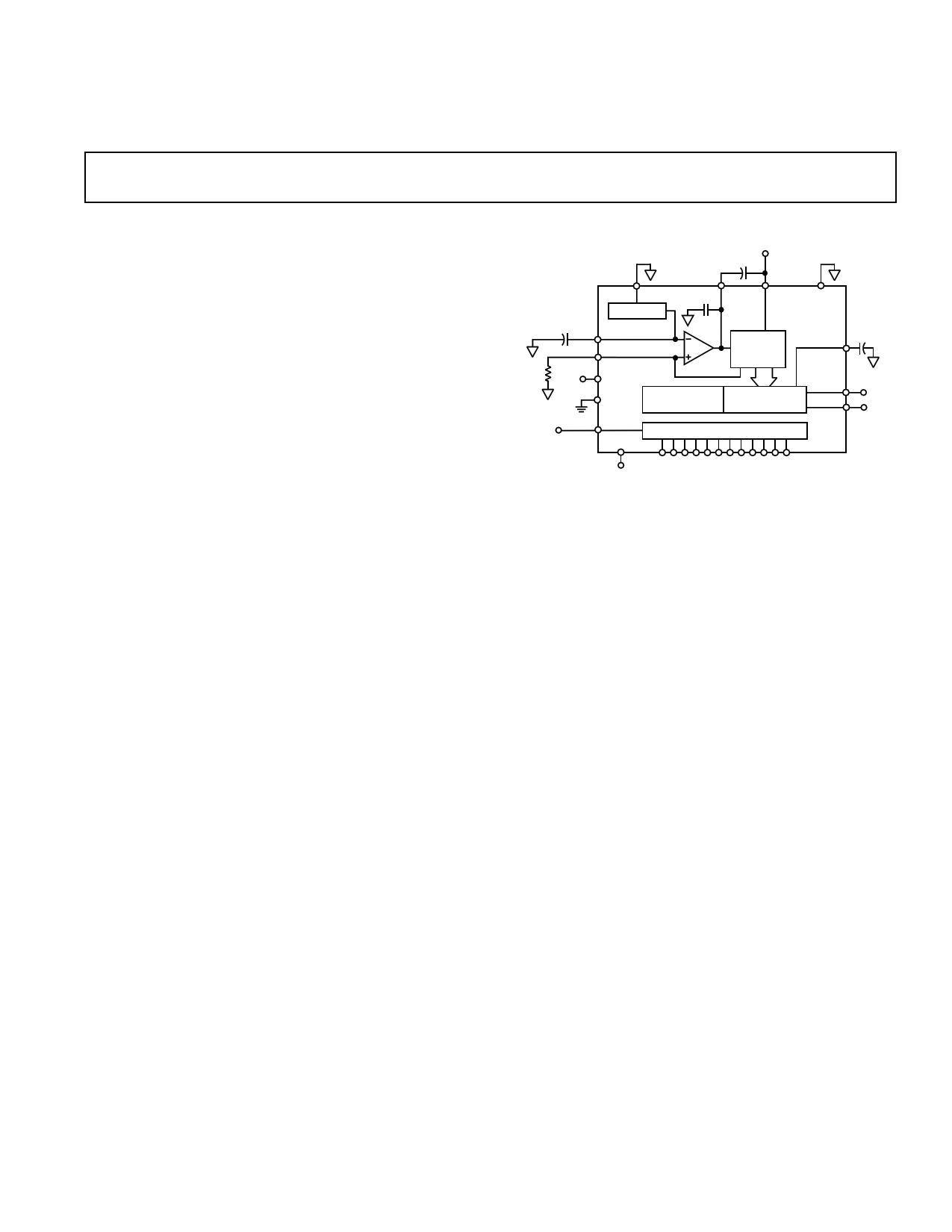
FUNCTIONAL BLOCK DIAGRAM
+5V
0.1F
0.1F
RSET
+5V
CLOCK
REFLO
+1.20V REF
REFIO
FS ADJ
COMP1 AVDD ACOM
50pF
AD9762
CURRENT
SOURCE
ARRAY
COMP2 0.1F
DVDD
DCOM
SEGMENTED
SWITCHES
LSB
SWITCHES
IOUTA
IOUTB
CLOCK
SLEEP
LATCHES
DIGITAL DATA INPUTS (DB11–DB0)
Differential current outputs are provided to support single-
ended or differential applications. Matching between the two
current outputs ensures enhanced dynamic performance in a
differential output configuration. The current outputs may be
tied directly to an output resistor to provide two complemen-
tary, single-ended voltage outputs or fed directly into a trans-
former. The output voltage compliance range is 1.25 V.
The on-chip reference and control amplifier are configured for
maximum accuracy and flexibility. The AD9762 can be driven
by the on-chip reference or by a variety of external reference
voltages. The internal control amplifier which provides a wide
(>10:1) adjustment span allows the AD9762 full-scale current
to be adjusted over a 2 mA to 20 mA range while maintaining
excellent dynamic performance. Thus, the AD9762 may oper-
ate at reduced power levels or be adjusted over a 20 dB range to
provide additional gain ranging capabilities.
The AD9762 is available in 28-lead SOIC and TSSOP pack-
ages. It is specified for operation over the industrial tempera-
ture range.
PRODUCT HIGHLIGHTS
1. The AD9762 is a member of the TxDAC product family which
provides an upward or downward component selection path
based on resolution (8 to 14 bits), performance and cost.
2. Manufactured on a CMOS process, the AD9762 uses a pro-
prietary switching technique that enhances dynamic perfor-
mance beyond what was previously attainable by higher
power/cost bipolar or BiCMOS devices.
3. On-chip, edge-triggered input CMOS latches interface readily
to +3 V and +5 V CMOS logic families. The AD9762 can
support update rates up to 125 MSPS.
4. A flexible single-supply operating range of 2.7 V to 5.5 V and
a wide full-scale current adjustment span of 2 mA to 20 mA
allow the AD9762 to operate at reduced power levels.
5. The current output(s) of the AD9762 can be easily config-
ured for various single-ended or differential circuit topologies.
One Technology Way, P.O. Box 9106, Norwood, MA 02062-9106, U.S.A.
Tel: 781/329-4700 World Wide Web Site: http://www.analog.com
Fax: 781/326-8703
© Analog Devices, Inc., 2000
1 page 
PIN CONFIGURATION
(MSB) DB11 1
28 CLOCK
DB10 2
27 DVDD
DB9 3
26 DCOM
DB8 4
25 NC
DB7 5 AD9762 24 AVDD
DB6 6 TOP VIEW 23 COMP2
DB5 7 (Not to Scale) 22 IOUTA
DB4 8
21 IOUTB
DB3 9
20 ACOM
DB2 10
19 COMP1
DB1 11
18 FS ADJ
DB0 12
17 REFIO
NC 13
16 REFLO
NC 14
15 SLEEP
NC = NO CONNECT
AD9762
PIN DESCRIPTIONS
Pin No. Name
Description
1
DB11
Most Significant Data Bit (MSB).
2–11
DB10–DB1 Data Bits 1–10.
12 DB0 Least Significant Data Bit (LSB).
13, 14, 25 NC
No Internal Connection.
15
SLEEP
Power-down Control Input. Active High. Contains active pull-down circuit, thus may be left unterminated if
not used.
16 REFLO Reference Ground when Internal 1.2 V Reference Used. Connect to AVDD to disable internal reference.
17
REFIO
Reference Input/Output. Serves as reference input when internal reference disabled (i.e., Tie REFLO to
AVDD). Serves as 1.2 V reference output when internal reference activated (i.e., Tie REFLO to ACOM).
Requires 0.1 µF capacitor to ACOM when internal reference activated.
18 FS ADJ Full-Scale Current Output Adjust.
19 COMP1 Bandwidth/Noise Reduction Node. Add 0.1 µF to AVDD for optimum performance.
20 ACOM Analog Common.
21 IOUTB Complementary DAC Current Output. Full-scale current when all data bits are 0s.
22 IOUTA DAC Current Output. Full-scale current when all data bits are 1s.
23 COMP2 Internal Bias Node for Switch Driver Circuitry. Decouple to ACOM with 0.1 µF capacitor.
24
AVDD
Analog Supply Voltage (+2.7 V to +5.5 V).
26 DCOM Digital Common.
27
DVDD
Digital Supply Voltage (+2.7 V to +5.5 V).
28 CLOCK Clock Input. Data latched on positive edge of clock.
REV. B
–5–
5 Page 
AD9762
FUNCTIONAL DESCRIPTION
Figure 39 shows a simplified block diagram of the AD9762.
The AD9762 consists of a large PMOS current source array
that is capable of providing up to 20 mA of total current. The
array is divided into 31 equal currents that make up the 5
most significant bits (MSBs). The next 4 bits or middle bits
consist of 15 equal current sources whose value is 1/16th of an
MSB current source. The remaining LSBs are binary weighted
fractions of the middle-bits current sources. Implementing
the middle and lower bits with current sources, instead of an
R-2R ladder, enhances its dynamic performance for multitone
or low amplitude signals and helps maintain the DAC’s high
output impedance (i.e., >100 kΩ).
All of these current sources are switched to one or the other
of the two output nodes (i.e., IOUTA or IOUTB) via PMOS differen-
tial current switches. The switches are based on a new archi-
tecture that drastically improves distortion performance. This new
switch architecture reduces various timing errors and provides
matching complementary drive signals to the inputs of the
differential current switches.
The analog and digital sections of the AD9762 have separate
power supply inputs (i.e., AVDD and DVDD) that can operate
independently over a 2.7 volt to 5.5 volt range. The digital
section, which is capable of operating up to a 125 MSPS clock
rate, consists of edge-triggered latches and segment decoding
logic circuitry. The analog section includes the PMOS current
sources, the associated differential switches, a 1.20 V bandgap
voltage reference and a reference control amplifier.
The full-scale output current is regulated by the reference
control amplifier and can be set from 2 mA to 20 mA via an
external resistor, RSET. The external resistor, in combination
with both the reference control amplifier and voltage refer-
ence VREFIO, sets the reference current IREF, which is mirrored
over to the segmented current sources with the proper scaling
factor. The full-scale current, IOUTFS, is thirty-two times the value
of IREF.
DAC TRANSFER FUNCTION
The AD9762 provides complementary current outputs, IOUTA
and IOUTB. IOUTA will provide a near full-scale current output,
IOUTFS, when all bits are high (i.e., DAC CODE = 4095) while
IOUTB, the complementary output, provides no current. The
current output appearing at IOUTA and IOUTB is a function of
both the input code and IOUTFS and can be expressed as:
IOUTA = (DAC CODE/4096) × IOUTFS
(1)
IOUTB = (4095 – DAC CODE)/4096 × IOUTFS
(2)
where DAC CODE = 0 to 4095 (i.e., Decimal Representation).
As mentioned previously, IOUTFS is a function of the reference
current IREF, which is nominally set by a reference voltage
VREFIO and external resistor RSET. It can be expressed as:
IOUTFS = 32 × IREF
(3)
where IREF = VREFIO/RSET
(4)
The two current outputs will typically drive a resistive load
directly or via a transformer. If dc coupling is required, IOUTA
and IOUTB should be directly connected to matching resistive
loads, RLOAD, which are tied to analog common, ACOM. Note,
RLOAD may represent the equivalent load resistance seen by
IOUTA or IOUTB as would be the case in a doubly terminated
50 Ω or 75 Ω cable. The single-ended voltage output appearing
at the IOUTA and IOUTB nodes is simply :
VOUTA = IOUTA × RLOAD
(5)
VOUTB = IOUTB × RLOAD
(6)
Note the full-scale value of VOUTA and VOUTB should not exceed
the specified output compliance range to maintain specified
distortion and linearity performance.
The differential voltage, VDIFF, appearing across IOUTA and
IOUTB is:
VDIFF = (IOUTA – IOUTB) × RLOAD
(7)
Substituting the values of IOUTA, IOUTB, and IREF; VDIFF can be
expressed as:
VDIFF = {(2 DAC CODE – 4095)/4096} ×
(32 RLOAD/RSET) × VREFIO
(8)
These last two equations highlight some of the advantages of
operating the AD9762 differentially. First, the differential
operation will help cancel common-mode error sources associated
with IOUTA and IOUTB such as noise, distortion and dc offsets.
Second, the differential code dependent current and subsequent
voltage, VDIFF, is twice the value of the single-ended voltage
output (i.e., VOUTA or VOUTB), thus providing twice the signal
power to the load.
Note, the gain drift temperature performance for a single-ended
(VOUTA and VOUTB) or differential output (VDIFF) of the AD9762
can be enhanced by selecting temperature tracking resistors for
RLOAD and RSET due to their ratiometric relationship as shown
in Equation 8.
+5V
0.1F
REV. B
0.1F
VREFIO
RSET
2k⍀
CLOCK
IREF
+5V
REFLO
COMP1 AVDD
ACOM
+1.20V REF
REFIO
FS ADJ
50pF
AD9762
PMOS
CURRENT SOURCE
ARRAY
COMP2
DVDD
DCOM
SEGMENTED SWITCHES
FOR DB11–DB3
LSB
SWITCHES
IOUTA
IOUTB
CLOCK
SLEEP
LATCHES
0.1F
IOUTB
VDIFF = VOUTA – VOUTB
IOUTA
VOUTB
RLOAD
50⍀
VOUTA
RLOAD
50⍀
DIGITAL DATA INPUTS (DB11–DB0)
Figure 39. Functional Block Diagram
–11–
11 Page | ||
| Páginas | Total 23 Páginas | |
| PDF Descargar | [ Datasheet AD9762.PDF ] | |
Hoja de datos destacado
| Número de pieza | Descripción | Fabricantes |
| AD976 | 16-Bit/ 100 kSPS/200 kSPS BiCMOS A/D Converters | Analog Devices |
| AD9760 | 10-Bit 125 MSPS TxDAC D/A Converter | Analog Devices |
| AD9761 | Dual 10-Bit TxDAC+ | Analog Devices |
| AD9762 | 12-Bit/ 125 MSPS TxDAC D/A Converter | Analog Devices |
| Número de pieza | Descripción | Fabricantes |
| SLA6805M | High Voltage 3 phase Motor Driver IC. |
Sanken |
| SDC1742 | 12- and 14-Bit Hybrid Synchro / Resolver-to-Digital Converters. |
Analog Devices |
|
DataSheet.es es una pagina web que funciona como un repositorio de manuales o hoja de datos de muchos de los productos más populares, |
| DataSheet.es | 2020 | Privacy Policy | Contacto | Buscar |