|
|
|
PDF LTM2895 Data sheet ( Hoja de datos )
| Número de pieza | LTM2895 | |
| Descripción | 100MHz Isolated DAC SPI Serial Interface | |
| Fabricantes | Linear Technology | |
| Logotipo | ||
Hay una vista previa y un enlace de descarga de LTM2895 (archivo pdf) en la parte inferior de esta página. Total 28 Páginas | ||
|
No Preview Available !
FEATURES
nn Isolated Interface: 6000VRMS for 1 Minute
nn UL-CSA-IEC Certification Pending
nn 100MHz SPI-Compatible I/O
nn Configurable SPI Word-Length: 8 to 32 Bits
nn Supports Two Isolated Chip Selects
nn Falling Edge Sensitive Low Jitter LOAD
nn Three Isolated Control or Multiplexer Signals
nn 1.71V to 5.5V I/O Voltages
nn 3V to 5.5V Supply Voltages
nn High Common Mode Transient Immunity
nn 15mm × 6.25mm BGA Package
APPLICATIONS
nn Remote Interface Control
nn Industrial Process Control and Automation
nn Test and Measurement Equipment
nn Breaking Ground Loops
LTM2895
100MHz Isolated
DAC SPI Serial Interface
DESCRIPTION
The LTM®2895 is a high speed isolated µModule® (micro-
module) SPI interface with DAC control signals designed
to isolate LTC’s family of general purpose DACs and to
isolate general purpose SPI interfaces. The LTM2895
works with DACs and general purpose devices that have
a mode (0, 0) SPI interface.
The interface enables fast data throughput, which makes
the LTM2895 ideally suited for a wide variety of applica-
tions. The high speed SPI-compatible serial port supports
1.71V to 5.5V logic supplies. The LTM2895 is targeted at
generic SPI and digital-to-analog converter applications.
The isolation barrier tolerates large voltage ground varia-
tions between the logic interface and the isolated side of
the LTM2895. Uninterrupted communication is maintained
during voltage transients greater than 50kV/µs.
L, LT, LTC, LTM, Linear Technology, the Linear logo and μModule are registered trademarks
and SoftSpan is a trademark of Linear Technology Corporation. All other trademarks are the
property of their respective owners.
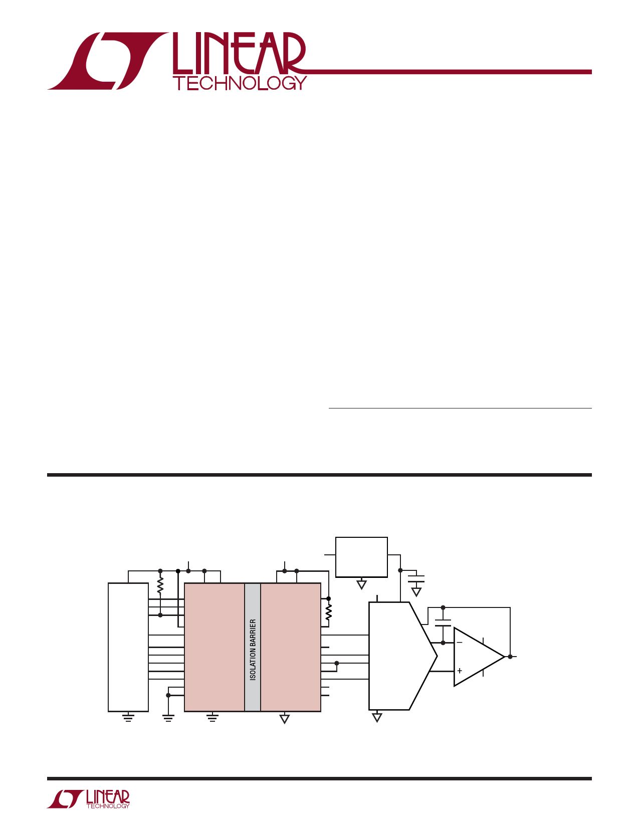
TYPICAL APPLICATION
3.3V
VDD
ON
SYSINT
FLTINT
LOAD
μP
CS
CS2
SCK
MOSI
MISO
CLR
GND
10k VL VCC
ON
BUSY
FAULT
LOAD
SS
SSB
SCK
MOSI
MISO
SA
SB
SC
GND
LTC2642-16 DAC Isolation
5Vi 8Vi
VCC2 VL2
ON2
LTM2895
LOAD2
SS2
SSB2
SCK2
MOSI2
MISO2
SA2
SB2
SC2
GND2
2895 TA01
LT6654-5
VIN VOUT
GND
5Vi
10µF
100k
VDD REF
RFB
CS INV
SCK LTC2642-16
DIN VOUT
CLR
GND
27pF
– 8Vi
+ LT1468
–8Vi
CONFIGURATION REGISTERS: WRITE 0x30H AND 0x83H
SETS SCK2 TO 33MHz AND WORDLENGTH TO 16-BIT
Vi = ISOLATED VOLTAGE SUPPLY
OUT
For more information www.linear.com/LTM2895
2895f
1
1 page 
LTM2895
S WITCHING CHARACTERISTICS The l denotes specifications that apply over the full specified operating
temperature range, otherwise specifications
GND2 = 0V; unless otherwise noted.
are
at
TA
=
25°C,
CL
=
20pF,
VCC
=
5V,
VL
=
3.3V,
GND
=
0V,
VCC2
=
5V,
VL2
=
3.3V,
SYMBOL
PARAMETER
tDLYSCKMOSI2
tDLYMOSI2SCK2
tSSSPACE
tSS2FSCK2
tSCK2SS2DIS
Delay SCK↑ to MOSI2 Valid
Setup MOSI2 to SCK2↑
SS↑ or SSB↑ Space to SS↓ or SSB↓
SS2↓ or SSB2↓ Delay to SCK2↑
Last SCK2↑ to SS2↑ or SSB2↑
MISO Rise/Fall Time
LOAD2, SS2, SSB2, MOSI2, SCK2 Rise/Fall
Time
Select Signals
SA, SB, SC Propagation Delay
SA2, SB2, SC2 Rise/Fall Time
CONDITIONS
(Note 2)
SCK2 Frequency 50MHz
SCK2 Frequency 50MHz
(Note 7)
(Note 7)
1.71V ≤ VL ≤ 5.5V
1.71V ≤ VL2 ≤ 5.5V
MIN TYP MAX UNITS
24 ns
l 1.5
ns
l 60
ns
l 45
ns
l 32
ns
500 ps
500 ps
l 40
l
80 150
10 20
ns
ns
I SOLATION CHARACTERISTICS TA = 25°C
SYMBOL PARAMETER
CONDITIONS
MIN TYP MAX
UNITS
VISO
Rated Dielectric Insulation Voltage
1 Minute, Derived from 1 Second
(Notes 4, 5, 6)
1 Second
6000
7200
Common Mode Transient Immunity
VCC = VL = ON = 5V to GND, VCC2 = VL2 =
ON2 = 5V to GND2, 1000V in 20ns
Transient Between GND and GND2 (Note 7)
50
100
VRMS
VRMS
kV/μs
VIORM
CTI
Maximum Working Insulation Voltage
Partial Discharge
Comparative Tracking Index
Depth of Erosion
(Note 2)
VPD = 1830VPEAK (Note 4)
IEC 60112 (Note 2)
IEC 60112 (Note 2)
1000
690
600
0.017
VPEAK, VDC
VRMS
5 pC
VRMS
mm
DTI Distance Through Insulation
(Note 2)
0.2 mm
Input to Output Resistance
(Notes 2, 4)
15
TΩ
Input to Output Capacitance
(Notes 2, 4)
3 pF
Creepage Distance
(Note 2)
9.2 mm
Note 1. Stresses beyond those listed under Absolute Maximum Ratings
may cause permanent damage to the device. Exposure to any Absolute
Maximum Rating condition for extended periods may affect device
reliability and lifetime.
Note 2. Guaranteed by design, not production tested.
Note 3. Maximum data rate is guaranteed by other measured parameters
and is not directly tested.
Note 4. Device considered a 2-terminal device. Measurement between
groups of pins A1 through C6 shorted together and pins N1 through R6
shorted together.
Note 5. The rated dielectric insulation voltage should not be interpreted as
a continuous voltage rating.
Note 6. In accordance with UL1577, each device is proof tested for the
6000VRMS rating by applying an RMS voltage multiplied by an acceleration
factor of 1.2 for one second.
Note 7. Evaluated by Design, not production tested.
Note 8. See Table 4 and Table 5 for minimum and maximum timing
specifications affected by the selection of SCK2 frequencies in the
configuration register.
Note 9. All currents into device pins are positive; all currents out of device
are negative. All voltages are referenced to their corresponding ground
unless otherwise specified.
Note 10. Continuous operation above specified maximum operating
junction temperature may result in device degradation or failure.
For more information www.linear.com/LTM2895
2895f
5
5 Page 
LTM2895
APPLICATIONS INFORMATION
OVERVIEW
The LTM2895 μModule transceiver provides a galvani-
cally isolated robust SPI interface including decoupling
capacitors. This flexible device can support a variety of
configurations and SCK frequencies. The LTM2895 is
ideal for breaking ground loops, noise isolation, protecting
equipment, or level shifting to a different ground refer-
ence. Error free operation is maintained through common
mode events exceeding 50kV/µs, providing excellent noise
isolation.
The LTM2895 can drop into most 4-wire SPI applica-
tions from 500kHz to 50MHz, without any configuration
required. To meet the specific needs of other SPI and DAC
applications, the LTM2895 can be personalized with a
configuration register allowing eight frequency and eight
word-length choices. The LTM2895 operates as a slave SPI
interface on the logic side and as a master SPI interface
on the isolated side. Only the necessary signal edges are
transferred across the isolation barrier and the SPI pat-
tern is recreated on the isolated side. Data read back from
the isolated side is temporarily stored in a buffer and the
result is delayed by one word-length. See Figure 9 for a
timing diagram of the SPI interface across the LTM2895.
Additional isolated signals are included to support features
of an isolated SPI device. DACs that support a LOAD DAC
input can use the low jitter LOAD signal for updating their
outputs. Reset, clear, or multiplexer functions are sup-
ported with the bidirectional select signals SA, SB, and SC.
A fault detection system watches for errors in input condi-
tions and isolated data corruption and reports on a single
open drain FAULT output.
ISOLATOR μModule TECHNOLOGY
The LTM2895 utilizes isolator μModule technology to trans-
late signals across an isolation barrier. Signals on either
side of the barrier are encoded into pulses and translated
across the isolation boundary using differential signaling
through coreless transformers formed in the μModule
substrate. This system, complete with error checking, fault
detection on fail, and extremely high common mode im-
munity, provides a robust solution for bidirectional signal
isolation. The μModule technology provides the means to
combine the isolated signaling with our SPI transceiver
in one small package.
SPI REQUIREMENTS
The SPI bus lacks a formal standard and, therefore, various
implementations of protocol, bit lengths, and signal polari-
ties exist. In the universe of devices with serial peripheral
interfaces (SPI), a nominal set of requirements must be
met to operate properly with the LTM2895. The signal flow
of a standard SPI protocol is used with a requirement that
the SS (Chip Select) signal frames the transaction. The
LTM2895 supports SPI mode (0, 0), where SCK captures
on the rising edge (CPHA = 0) and SCK starts low and
transitions high (CPOL = 0).
The following list summarizes the requirements for using
the LTM2895.
n Configure the SCK2 frequency to the master and ap-
plication device requirements
n SPI operates in mode (0, 0) (rising edge SCK captures data)
n Chip Select signal (SS or SSB) frames SPI pattern and
meets watchdog timeout requirements
First, the SCK2 frequency is selected to operate with the
device connected to the isolated side of the LTM2895.
The SCK2 frequency sets the low time of the clock signal
(tSCK2L) out of the LTM2895 and into the isolated SPI
interface. See section SCK2 FREQUENCY for specific
timing information. The master SCK frequency must be
equal or slower than the SCK2 frequency and greater than
the watchdog timeout.
Second, the LTM2895 logic side operates in mode (0,
0) with a variation on which edge of the SCK data shifts
out on. For configured SCK2 frequencies of 100MHz and
66MHz, the MOSI data is captured and the MISO data is
shifted on the rising edge of SCK, as shown in Figure 2.
This variation allows for additional propagation and setup
time to the next rising clock (SCK) edge. All setup and
hold timing characteristics are related to the rising edge of
the SCK. For configured SCK2 frequencies of 50MHz and
lower, MOSI is captured on the rising edge and MISO is
shifted on the falling edge of SCK, as shown in Figure 3.
For more information www.linear.com/LTM2895
2895f
11
11 Page | ||
| Páginas | Total 28 Páginas | |
| PDF Descargar | [ Datasheet LTM2895.PDF ] | |
Hoja de datos destacado
| Número de pieza | Descripción | Fabricantes |
| LTM2892 | SPI/Digital or I2C uModule Isolator | Linear Technology |
| LTM2895 | 100MHz Isolated DAC SPI Serial Interface | Linear Technology |
| Número de pieza | Descripción | Fabricantes |
| SLA6805M | High Voltage 3 phase Motor Driver IC. |
Sanken |
| SDC1742 | 12- and 14-Bit Hybrid Synchro / Resolver-to-Digital Converters. |
Analog Devices |
|
DataSheet.es es una pagina web que funciona como un repositorio de manuales o hoja de datos de muchos de los productos más populares, |
| DataSheet.es | 2020 | Privacy Policy | Contacto | Buscar |