|
|
|
PDF CY7C1020DV33 Data sheet ( Hoja de datos )
| Número de pieza | CY7C1020DV33 | |
| Descripción | 512 K (32 K x 16) Static RAM | |
| Fabricantes | Cypress Semiconductor | |
| Logotipo | ||
Hay una vista previa y un enlace de descarga de CY7C1020DV33 (archivo pdf) en la parte inferior de esta página. Total 13 Páginas | ||
|
No Preview Available !
CY7C1020DV33
512 K (32 K x 16) Static RAM
Features
■ Pin-and function-compatible with CY7C1020CV33
■ High speed
❐ tAA = 10 ns
■ Low active power
❐ ICC = 60 mA @ 10 ns
■ Low CMOS standby power
❐ ISB2 = 3 mA
■ 2.0 V Data retention
■ Automatic power-down when deselected
■ CMOS for optimum speed/power
■ Independent control of upper and lower bits
■ Available in Pb-free 44-pin 400-Mil wide Molded SOJ and
44-pin TSOP II packages
Functional Description
The CY7C1020DV33 is a high-performance CMOS static
RAM organized as 32,768 words by 16 bits. This device has
an automatic power-down feature that significantly reduces
power consumption when deselected.
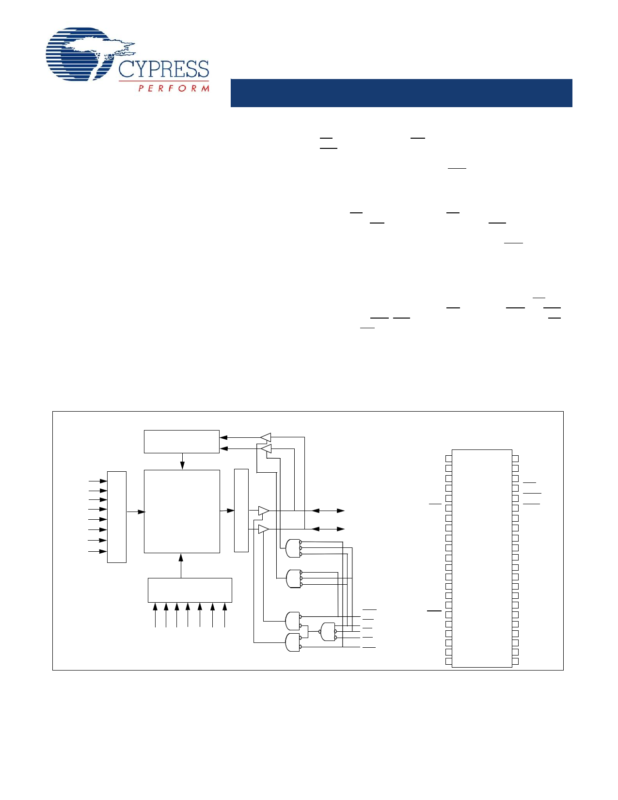
Logic Block Diagram
DATA IN DRIVERS
A7
A6
A5
A4
32K x 16
A3 RAM Array
A2
A1
A0
COLUMN DECODER
Writing to the device is accomplished by taking chip enable
(CE) and write enable (WE) inputs LOW. If byte low enable
(BLE) is LOW, then data from I/O pins (I/O0 through I/O7), is
written into the location specified on the address pins (A0
through A14). If byte high enable (BHE) is LOW, then data from
I/O pins (I/O8 through I/O15) is written into the location
specified on the address pins (A0 through A14).
Reading from the device is accomplished by taking chip
enable (CE) and output enable (OE) LOW while forcing the
write enable (WE) HIGH. If byte low enable (BLE) is LOW, then
data from the memory location specified by the address pins
will appear on I/O0 to I/O7. If byte high enable (BHE) is LOW,
then data from memory will appear on I/O8 to I/O15. See the
truth table at the back of this data sheet for a complete
description of read and write modes.
The input/output pins (I/O0 through I/O15) are placed in a
high-impedance state when the device is deselected (CE
HIGH), the outputs are disabled (OE HIGH), the BHE and BLE
are disabled (BHE, BLE HIGH), or during a write operation (CE
LOW, and WE LOW).
The CY7C1020DV33 is available in Pb-free 44-pin 400-Mil
wide Molded SOJ and 44-pin TSOP II packages.
For a complete list of related documentation, click here.
I/O0–I/O7
I/O8–I/O15
BHE
WE
CE
OE
BLE
Pin Configuration[1]
SOJ/TSOP II
Top View
NC
A3
A2
A1
A0
CE
I/O0
I/O1
I/O2
I/O3
VCC
VSS
I/O4
I/O5
I/O6
I/O7
WE
A4
A14
A13
A12
NC
1
2
3
4
5
6
7
8
9
10
11
12
13
14
15
16
17
18
19
20
21
22
44 A5
43 A6
42 A7
41 OE
40 BHE
39 BLE
38 I/O15
37 I/O14
36 I/O13
35 I/O12
34 VSS
33 VCC
32 I/O11
31 I/O10
30 I/O9
29 I/O8
28 NC
27 A8
26 A9
25 A10
24 A11
23 NC
Notes
1. NC pins are not connected on the die.
Cypress Semiconductor Corporation • 198 Champion Court
Document Number: 38-05461 Rev. *I
• San Jose, CA 95134-1709 • 408-943-2600
Revised November 19, 2014
1 page 
CY7C1020DV33
Data Retention Characteristics (Over the Operating Range)
Parameter
Description
Conditions
VDR
ICCDR
tCDR [3]
tR[12]
VCC
Data retention current
Chip deselect to data retention time
VCC = VDR = 2.0 V, CE > VCC – 0.3 V, Industrial
VIN > VCC – 0.3 V or VIN < 0.3 V
Operation recovery time
Data Retention Waveform
Min.
2.0
Max.
3
Unit
V
mA
0 ns
tRC ns
DATA RETENTION MODE
VCC
3.0 V
VDR > 2 V
3.0 V
tCDR
tR
CE
Switching Waveforms
Read Cycle No. 1 (Address Transition Controlled)[13, 14]
ADDRESS
DATA I/O
tOHA
PREVIOUS DATA VALID
tAA
tRRCC
Read Cycle No. 2 (OE Controlled)[14, 15]
DATA OUT VALID
ADDRESS
CE
OE
BHE, BLE
DATA I/O
VCC
SUPPLY
CURRENT
tACE
tDOE
tLZOE
tDBE
tLZBE
HIGH IMPEDANCE
tLZCE
tPU
50%
tRC
tHZOE
DATA OUT VALID
tHZCE
tHZBE
HIGH
IMPEDANCE
tPD
50%
ICC
ISB
Notes:
12. Full device operation requires linear VCC ramp from VDR to VCC(min.) > 50 s or stable at VCC(min.) > 50 s.
13. Device is continuously selected. OE, CE, BHE and/or BLE = VIL.
14. WE is HIGH for Read cycle.
15. Address valid prior to or coincident with CE transition LOW.
Document Number: 38-05461 Rev. *I
Page 5 of 13
5 Page 
Acronyms
Acronym
BHE
BLE
CE
CMOS
I/O
OE
SRAM
TSOP
WE
Description
byte high enable
byte low enable
chip enable
complementary metal oxide semiconductor
input/output
output enable
static random access memory
thin small outline package
write enable
Document Conventions
Units of Measure
Symbol
°C
A
mA
MHz
ns
pF
V
W
Unit of Measure
degrees Celsius
microamperes
milliamperes
megahertz
nanoseconds
picofarads
volts
ohms
watts
CY7C1020DV33
Document Number: 38-05461 Rev. *I
Page 11 of 13
11 Page | ||
| Páginas | Total 13 Páginas | |
| PDF Descargar | [ Datasheet CY7C1020DV33.PDF ] | |
Hoja de datos destacado
| Número de pieza | Descripción | Fabricantes |
| CY7C1020DV33 | 512 K (32 K x 16) Static RAM | Cypress Semiconductor |
| Número de pieza | Descripción | Fabricantes |
| SLA6805M | High Voltage 3 phase Motor Driver IC. |
Sanken |
| SDC1742 | 12- and 14-Bit Hybrid Synchro / Resolver-to-Digital Converters. |
Analog Devices |
|
DataSheet.es es una pagina web que funciona como un repositorio de manuales o hoja de datos de muchos de los productos más populares, |
| DataSheet.es | 2020 | Privacy Policy | Contacto | Buscar |