|
|
|
PDF IDT709089L Data sheet ( Hoja de datos )
| Número de pieza | IDT709089L | |
| Descripción | HIGH-SPEED 64K x 8 SYNCHRONOUS DUAL-PORT STATIC RAM | |
| Fabricantes | Integrated Device Technology | |
| Logotipo | ||
Hay una vista previa y un enlace de descarga de IDT709089L (archivo pdf) en la parte inferior de esta página. Total 17 Páginas | ||
|
No Preview Available !
HIGH-SPEED 64K x 8
SYNCHRONOUS
DUAL-PORT STATIC RAM
PRELIMINARY
IDT709089S/L
Features:
x True Dual-Ported memory cells which allow simultaneous
access of the same memory location
x High-speed clock to data access
– Commercial: 9/12/15ns (max.)
x Low-power operation
– IDT709089S
Active: 950mW (typ.)
Standby: 5mW (typ.)
– IDT709089L
Active: 950mW (typ.)
Standby: 1mW (typ.)
x Flow-Through or Pipelined output mode on either port via
the FT/PIPE pin
x Counter enable and reset features
x Dual chip enables allow for depth expansion without
additional logic
x Full synchronous operation on both ports
– 4ns setup to clock and 1ns hold on all control, data,
and address inputs
– Data input, address, and control registers
– Fast 9ns clock to data out in the Pipelined output mode
– Self-timed write allows fast cycle time
– 15ns cycle time, 66MHz operation in the Pipelined
output mode
x TTL- compatible, single 5V (±10%) power supply
x Industrial temperature range (–40°C to +85°C) is available
for selected speeds
x Available in 100-pin Thin Quad Flatpack (TQFP) package
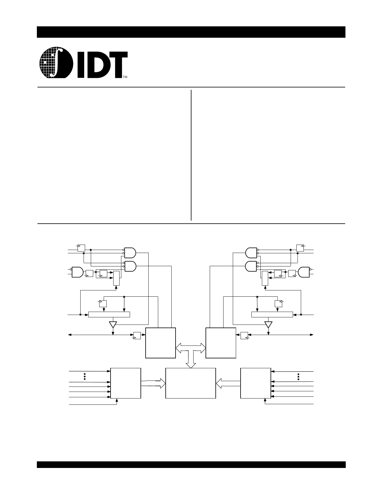
Functional Block Diagram
R/WL
OEL
CE0L
CE1L
1
0
0/1
R/WR
OER
CE0R
1 CE1R
0
0/1
FT/PIPEL
I/O0L - I/O7L
A15L
A0L
CLKL
ADSL
CNTENL
CNTRSTL
0/1 1
0
I/O
Control
I/O
Control
0 1 0/1
Counter/
Address
Reg.
MEMORY
ARRAY
Counter/
Address
Reg.
FT/PIPER
I/O0R - I/O7R
A15R
A0R
CLKR
ADSR
CNTENR
CNTRSTR
3242 drw 01
©2000 Integrated Device Technology, Inc.
1
FEBRUARY 2000
DSC-3242/10
1 page 
IDT709089S/L
High-Speed 64K x 8 Synchronous Dual-Port Static RAM
Preliminary
Industrial and Commercial Temperature Ranges
DC Electrical Characteristics Over the Operating
Temperature and Supply Voltage Range (VCC = 5.0V ± 10%)
709089S/L
Symbol
Parameter
Test Conditions
Min. Max. Unit
|ILI| Input Leakage Current(1)
VCC = 5.5V, VIN = 0V to VCC
___ 10 µ A
|ILO| Output Leakage Current
CE0 = VIH or CE1 = VIL, VOUT = 0V to VCC
___ 10 µ A
VOL Output Low Voltage
IOL = +4mA
___ 0.4 V
VOH Output High Voltage
IOH = -4mA
2.4 ___ V
NOTE:
1. At Vcc < 2.0V input leakages are undefined.
3242 tbl 08
DC Electrical Characteristics Over the Operating
Temperature and Supply Voltage Range(6,7) (VCC = 5V ± 10%)
709089X9
Com'l Only
709089X12
Com'l Only
709089X15
Com'l Only
Symbol
Parameter
Test Condition
Version
Typ.(4) Max. Typ.(4) Max. Typ.(4) Max. Unit
ICC Dynamic Operating
Current
(Both Ports Active)
CEL and CER= VIL
Outputs Open
f = fMAX(1)
COM'L S 210 390 200 345 190 325 mA
L 210 350 200 305 190 285
IND
S ____ ____ ____ ____ ____ ____
L ____ ____ ____ ____ ____ ____
ISB1 Standby Current
(Both Ports - TTL
Level Inputs)
CEL = CER = VIH
f = fMAX(1)
COM'L
IND
S
L
S
L
50
50
____
____
135 50
115 50
____ ____
____ ____
100 50
90 50
____ ____
____ ____
110 mA
90
____
____
ISB2 Standby Current
(One Port - TTL
Level Inputs)
CE"A" = VIL and
CE"B" = VIH(3)
Active Port Outputs
Open,
f=fMAX(1)
COM'L S 140 270 130 230 120 220 mA
L 140 240 130 200 120 190
IND
S ____ ____ ____ ____ ____ ____
L ____ ____ ____ ____ ____ ____
ISB3 Full Standby Current
(Both Ports -
CMOS Level Inputs)
Both Ports CER and
CEL > VCC - 0.2V
VIN > VCC - 0.2V or
VIN < 0.2V, f = 0(2)
COM'L S 1.0 15 1.0 15 1.0 15 mA
L 0.2 5 0.2 5 0.2 5
IND
S ____ ____ ____ ____ ____ ____
L ____ ____ ____ ____ ____ ____
ISB4 Full Standby Current
(One Port -
CMOS Level Inputs)
CE"A" < 0.2V and
CE"B" > VCC - 0.2V(5)
VIN > VCC - 0.2V or
VIN < 0.2V, Active Port
Outputs Open, f = fMAX(1)
COM'L S 130 245 120 205 110 195 mA
L 130 225 120 185 110 175
IND
S ____ ____ ____ ____ ____ ____
L ____ ____ ____ ____ ____ ____
NOTES:
3242 tbl 09
1. At f = fMAX, address and control lines (except Output Enable) are cycling at the maximum frequency clock cycle of 1/tCYC, using "AC TEST CONDITIONS" at input levels of
GND to 3V.
2. f = 0 means no address, clock, or control lines change. Applies only to input at CMOS level standby.
3. Port "A" may be either left or right port. Port "B" is the opposite from port "A".
4. Vcc = 5V, TA = 25°C for Typ, and are not production tested. ICC DC(f=0) = 150mA (Typ).
5. CEX = VIL means CE0X = VIL and CE1X = VIH
CEX = VIH means CE0X = VIH or CE1X = VIL
CEX < 0.2V means CE0X < 0.2V and CE1X > VCC - 0.2V
CEX > VCC - 0.2V means CE0X > VCC - 0.2V or CE1X < 0.2V
"X" represents "L" for left port or "R" for right port.
6. 'X' in part numbers indicate power (S or L).
7. Industrial temperature: for specific speeds, packages and powers contact your sales office.
6.542
5 Page 
IDT709089S/L
High-Speed 64K x 8 Synchronous Dual-Port Static RAM
Preliminary
Industrial and Commercial Temperature Ranges
Timing Waveform of Pipelined Read-to-Write-to-Read (OE = VIL)(3)
tCYC2
tCH2
tCL2
CLK
CE0
CE1
tSC tHC
R/W
tSW tHW
tSW tHW
(4)
ADDRESS
DATAIN
DATAOUT
An
tSA tHA
An +1
tCD2
(2)
READ
An + 2
An + 2
tSD tHD
An + 3
Dn + 2
tCKHZ (1)
Qn
NOP(5)
WRITE
An + 4
tCKLZ(1)
tCD2
Qn + 3
READ
3242 drw 11
Timing Waveform of Pipelined Read-to-Write-to-Read (OE Controlled)(3)
tCYC2
tCH2
tCL2
CLK
CE0
tSC tHC
CE1
R/W
tSW tHW
tSW tHW
ADDRESS(4)
DATAIN
DATAOUT
An
tSA tHA
(2)
An +1
An + 2
tSD tHD
tCD2
Dn + 2
Qn
tOHZ(1)
An + 3
Dn + 3
An + 4
An + 5
tCKLZ(1)
tCD2
Qn + 4
OE
READ
WRITE
READ
3242 drw 12
NOTES:
1. Transition is measured 0mV from Low or High-impedance voltage with the Output Test Load (Figure 2).
2. Output state (High, Low, or High-impedance) is determined by the previous cycle control signals.
3. CE0 and ADS = VIL; CE1, CNTEN, and CNTRST = VIH.
4. Addresses do not have to be accessed sequentially since ADS = VIL constantly loads the address on the rising edge of the CLK; numbers are for reference use only.
5. "NOP" is "No Operation." Data in memory at the selected address may be corrupted and should be re-written to guarantee data integrity.
61.412
11 Page | ||
| Páginas | Total 17 Páginas | |
| PDF Descargar | [ Datasheet IDT709089L.PDF ] | |
Hoja de datos destacado
| Número de pieza | Descripción | Fabricantes |
| IDT709089L | HIGH-SPEED 64K x 8 SYNCHRONOUS DUAL-PORT STATIC RAM | Integrated Device Technology |
| IDT709089S | HIGH-SPEED 64K x 8 SYNCHRONOUS DUAL-PORT STATIC RAM | Integrated Device Technology |
| Número de pieza | Descripción | Fabricantes |
| SLA6805M | High Voltage 3 phase Motor Driver IC. |
Sanken |
| SDC1742 | 12- and 14-Bit Hybrid Synchro / Resolver-to-Digital Converters. |
Analog Devices |
|
DataSheet.es es una pagina web que funciona como un repositorio de manuales o hoja de datos de muchos de los productos más populares, |
| DataSheet.es | 2020 | Privacy Policy | Contacto | Buscar |