|
|
|
PDF BU90T82 Data sheet ( Hoja de datos )
| Número de pieza | BU90T82 | |
| Descripción | 27bit LVDS Dual-out Transmitter | |
| Fabricantes | ROHM Semiconductor | |
| Logotipo | ||
Hay una vista previa y un enlace de descarga de BU90T82 (archivo pdf) en la parte inferior de esta página. Total 29 Páginas | ||
|
No Preview Available !
Datasheet
LVDS Interface LSI
27bit LVDS Dual-out Transmitter
BU90T82
General Description
The BU90T82 transmitter operates from 10MHz to
174MHz wide clock range, and 27bits data of parallel
CMOS level inputs (R/G/B24bits and VSYNC, HSYNC,
DE) are converted to eight channels of LVDS data
stream. Data is transmitted seven times (7X) stream and
reduce cable number by 3(1/3) or less.
The BU90T82 has low swing mode to be able to expect
further low power and low EMI.
Flexible Input/Output mode support various application
interfaces.
Features
■ 27bits data of parallel LVCMOS level inputs are
converted to 4 or 8 channels of LVDS data stream.
■ The maximum data rate is 1218Mbps/Lane
■ Support clock frequency from 10MHz up to 174MHz
■ Flexible Input/Output mode
1. Single in / Single LVDS out
2. Single in / Dual LVDS out
3. Double edge Single in / Dual LVDS out
4. Single in / Distribution LVDS out
Key Specifications
■ Supply Voltage Range VDD
VDDIO
■ Operating Frequency
■ Operating Temperature Range
1.62 to 1.98 V
1.62 to 3.60 V
10 to 174 MHz
-40 to +85 ℃
●Package
SBGA072T070A
(Typ) (Typ) (Max)
7.0mm×7.0mm×1.2mm
●Applications
■ Security camera, Digital camera
■ Tablet
■ Flat Panel Display
■ Power down mode
■ Clock edge selectable
■ 6bit/8bit mode selectable
■ LVDS output mapping selectable (VESA/JIEDA)
■ Support reduced swing LVDS for low EMI
■ Support LVDS Outputs pin reverse function
■ Support spread spectrum clock generator input
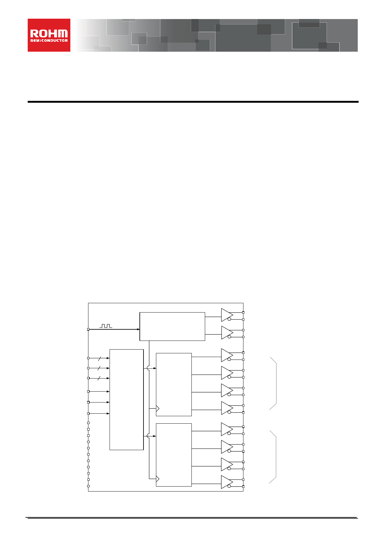
Block Diagram
LVCMOS Input
CLKIN
(10MHz - 174MHz)
TCLK1 +/-
LVDS Output
PLL
TCLK2 +/-
(10MHz - 174MHz)
R1[7:0]
G1[7:0]
B1[7:0]
HSYNC
VSYNC
DE
PWDN
OE
RS
RF
6B8B
MAP
MODE
DDRN
FLIP
PRBS
TEST
8
8
8
Data Mapping
Parallel to Serial
Converter
Parallel to Serial
Converter
TA1 +/-
TB1 +/-
TC1 +/-
TD1 +/-
LVDS Channel1
TA2 +/-
TB2 +/-
TC2 +/-
TD2 +/-
LVDS Channel2
Figure 1. Block Diagram
〇Product structure : Silicon monolithic integrated circuit
.www.rohm.com
© 2014 ROHM Co., Ltd. All rights reserved.
TSZ22111 • 14 • 001
〇This product has no designed protection against radioactive rays
1/25
TSZ02201-0L2L0H500270-1-2
06.July.2016 Rev.003
1 page 
BU90T82
Datasheet
Pin Description
Pin name
TA1+/-, TB1+/-,
TC1+/-,TD1+/-
TCLK1+/-
TA2+/-, TB2+/-,
TC2+/-,TD2+/-
TCLK2+/-
R1[7:0]
G1[7:0]
B1[7:0]
DE
HSYNC
VSYNC
Pin NO.
A1,B1,A2,B2,A3,B3,A5,B5
A4,B4
A6,B6,A7,B7,A8,B8,C9,C8
A9,B9
G1,G2,F1,F2,E1,E2,D1,D2
J4,H4,J3,H3,J2,H2,J1,H1
J8,H8,J7,H7,J6,H6,J5,H5
G9
J9
H9
Type
LVDS output
LVDS output
LVCMOS input
LVCMOS input
Descriptions
LVDS Data output (Channel1)
LVDS Clock output (Channel1)
LVDS Data output (Channel2)
LVDS Clock output (Channel2)
Pixel data input
Control data input
CLKIN
PWDN
OE
RF
RS
MAP
MODE
DDRN
6B8B
FLIP
TEST
F9
D8
D9
G8
F8
E8
E7
E9
F7
C2
C3
LVCMOS input Clock input
LVCMOS input
Power Down
H:Normal operation
L:Power down (all LVDS output signal are Hi-z)
LVDS Output Enable.
H: Output enable
L: Output disable(all LVDS output signal are Hi-z)
Input CLK Triggering Edge Select.
H:Rising edge
L:Falling edge
LVDS Swing Mode Select
H: 350mV
L: 200mV
LVDS Output Data Mapping Select
H: JEIDA
L: VESA
LVDS Output Mode Select
H: Single in / Single out
L: Single in / Dual out
(MODE=H, DDRN=L Distribution out)
Input CLK Triggering Edge Select.
H: DDR function disable
L: DDR function enable
(It is possible only at Dual-out mode)
(MODE=H, DDRN=L Distribution out)
6bit/8bit Mode Select
H : 6bit mode (TD1+/-, TD2+/- outputs are Hi-z)
L : 8bit mode
LVDS Output Pin Reverse Select.
H: Reverse
L/Open: Normal
TEST Mode Select (Normal operation is Low)
PRBS
C1
PRBS Data Output (Normal operation is Low)
VDD
VDDIO
C5,C7,D3,G3,G5
G7
Power
Power Supply for Internal Core
Power Supply for I/O
GND
C4,C6,D7,E3,F3,G4,G6
Ground
Ground Pins
www.rohm.com
© 2014 ROHM Co., Ltd. All rights reserved.
TSZ22111 • 15 • 001
5/25
TSZ02201-0L2L0H500270-1-2
06.July.2016 Rev.003
5 Page 
BU90T82
LVCMOS Data Inputs Pixel Map Table
Table 5. LVCMOS Data Inputs Pixel Map Table
TFT Panel Data
24Bit
18Bit (Map=L)
LSB R10
R10
R11 R11
R12 R12
R13 R13
R14 R14
R15 R15
R16 -
MSB
R17
-
LSB G10
G10
G11 G11
G12 G12
G13 G13
G14 G14
G15 G15
G16 -
MSB
G17
-
LSB B10
B10
B11 B11
B12 B12
B13 B13
B14 B14
B15 B15
B16 -
MSB
B17
-
VSYNC
VSYNC
HSYNC
HSYNC
DE DE
18Bit (Map=H)
-
-
R10
R11
R12
R13
R14
R15
-
-
G10
G11
G12
G13
G14
G15
-
-
B10
B11
B12
B13
B14
B15
VSYNC
HSYNC
DE
BU90T82 Input
R10
R11
R12
R13
R14
R15
R16
R17
G10
G11
G12
G13
G14
G15
G16
G17
B10
B11
B12
B13
B14
B15
B16
B17
VSYNC
HSYNC
DE
Datasheet
www.rohm.com
© 2014 ROHM Co., Ltd. All rights reserved.
TSZ22111 • 15 • 001
11/25
TSZ02201-0L2L0H500270-1-2
06.July.2016 Rev.003
11 Page | ||
| Páginas | Total 29 Páginas | |
| PDF Descargar | [ Datasheet BU90T82.PDF ] | |
Hoja de datos destacado
| Número de pieza | Descripción | Fabricantes |
| BU90T81 | 27bit LVDS Transmitter | ROHM Semiconductor |
| BU90T82 | 27bit LVDS Dual-out Transmitter | ROHM Semiconductor |
| Número de pieza | Descripción | Fabricantes |
| SLA6805M | High Voltage 3 phase Motor Driver IC. |
Sanken |
| SDC1742 | 12- and 14-Bit Hybrid Synchro / Resolver-to-Digital Converters. |
Analog Devices |
|
DataSheet.es es una pagina web que funciona como un repositorio de manuales o hoja de datos de muchos de los productos más populares, |
| DataSheet.es | 2020 | Privacy Policy | Contacto | Buscar |