|
|
|
PDF 9FGV0431 Data sheet ( Hoja de datos )
| Número de pieza | 9FGV0431 | |
| Descripción | 4-OUTPUT VERY LOW POWER PCIE GEN1-2-3 CLOCK GENERATOR | |
| Fabricantes | IDT | |
| Logotipo | ||
Hay una vista previa y un enlace de descarga de 9FGV0431 (archivo pdf) en la parte inferior de esta página. Total 15 Páginas | ||
|
No Preview Available !
4-OUTPUT VERY LOW POWER PCIE GEN1-2-3 CLOCK GENERATOR
DATASHEET
9FGV0431
Description
The 9FGV0431 is a 4-output very low power clock
generator for PCIe Gen 1, 2 and 3 applications. The device
has 4 output enables for clock management and supports 2
different spread spectrum levels in addition to spread off.
Recommended Application
PCIe Gen1-2-3 Clock Generator
Output Features
• 4 - 0.7V low-power HCSL-compatible (LP-HCSL) DIF
pairs
• 1 - 1.8V LVCMOS REF output w/Wake-On-Lan
Key Specifications
• DIF cycle-to-cycle jitter <50ps
• DIF output-to-output skew <50ps
• DIF phase jitter is PCIe Gen1-2-3 compliant
• REF phase jitter is < 1.5ps RMS
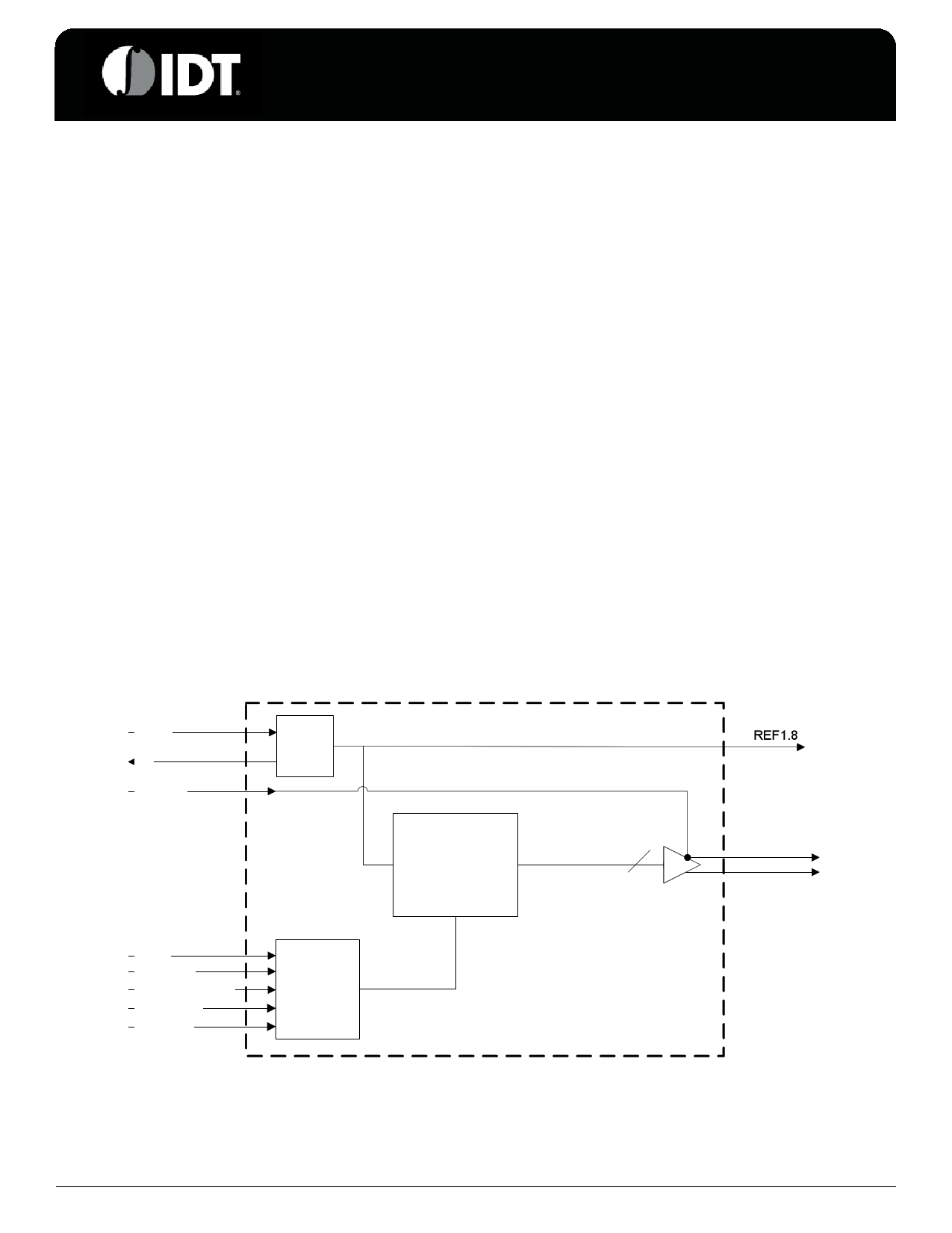
Block Diagram
Features/Benefits
• 1.8V operation; reduced power consuption
• OE# pins; support DIF power management
• LP-HCSL differential clock outputs; reduced power and
board space
• Programmable Slew rate for each output; allows tuning
for various line lengths
• Programmable output amplitude; allows tuning for
various application environments
• DIF outputs blocked until PLL is locked; clean system
start-up
• Selectable 0%, -0.25% or -0.5% spread on DIF outputs;
reduces EMI
• External 25MHz crystal; supports tight ppm with 0 ppm
synthesis error
• Configuration can be accomplished with strapping pins;
SMBus interface not required for device control
• 3.3V tolerant SMBus interface works with legacy
controllers
• Space saving 32-pin 5x5 mm MLF; minimal board space
• Selectable SMBus addresses; multiple devices can
easily share an SMBus segment
X1_25
X2
OE(3:0)#
OSC
SS Capable PLL
REF1.8
4
DIF(3:0)
SADR
SS_EN_tri
CKPWRGD_PD#
SDATA_3.3
SCLK_3.3
CONTROL
LOGIC
IDT® 4-OUTPUT VERY LOW POWER PCIE GEN1-2-3 CLOCK GENERATOR
1
9FGV0431 OCTOBER 18, 2016
1 page 
9FGV0431
4-OUTPUT VERY LOW POWER PCIE GEN1-2-3 CLOCK GENERATOR
Absolute Maximum Ratings
Stresses above the ratings listed below can cause permanent damage to the 9FGV0431. These ratings, which are standard
values for IDT commercially rated parts, are stress ratings only. Functional operation of the device at these or any other
conditions above those indicated in the operational sections of the specifications is not implied. Exposure to absolute
maximum rating conditions for extended periods can affect product reliability. Electrical parameters are guaranteed only over
the recommended operating temperature range.
PARAMETER
SYMBOL
CONDITIONS
1.8V Supply Voltage
VDDx1.8
Applies to All VDD pins
Input Voltage
VIN
Input High Voltage, SMBus VIHSMB
Storage Temperature
Ts
SMBus clock and data pins
Junction Temperature
Tj
Input ESD protection ESD prot
Human Body Model
1Guaranteed by design and characterization, not 100% tested in production.
2 Operation under these conditions is neither implied nor guaranteed.
3 Not to exceed 2.5V.
MIN
-0.5
-0.5
-65
2000
TYP
MAX
2.5
VDD+0.3V
3.6V
150
125
UNITS
V
V
V
°C
°C
V
NOTES
1,2
1, 3
1
1
1
1
Electrical Characteristics–Current Consumption
TA = TCOM or TIND; Supply Voltage per VDD of normal operation conditions, See Test Loads for Loading Conditions
PARAMETER
SYMBOL
CONDITIONS
MIN TYP MAX
IDDAOP
VDDA, All outputs active @100MHz
Operating Supply Current
IDDOP
VDD, All outputs active @100MHz
Suspend Supply Current
IDDSUSP
VDDxxx, PD# = 0, Wake-On-LAN enabled
Powerdown Current
IDDPD
PD#=0
1Guaranteed by design and characterization, not 100% tested in production.
2Assuming REF is not running in power down state
68
26 30
68
0.6 1
UNITS
mA
mA
mA
mA
NOTES
1
1
1
1, 2
Electrical Characteristics–Output Duty Cycle, Jitter, and Skew Characterisitics
TA = TCOM or TIND; Supply Voltage per VDD of normal operation conditions, See Test Loads for Loading Conditions
PARAMETER
SYMBOL
CONDITIONS
MIN TYP MAX
Duty Cycle
tDC Measured differentially, PLL Mode
Skew, Output to Output
tsk3
VT = 50%
Jitter, Cycle to cycle
tjcyc-cyc
PLL mode
1Guaranteed by design and characterization, not 100% tested in production.
2 Measured from differential waveform
45 50.1 55
37 50
12 50
UNITS
%
ps
ps
NOTES
1
1
1,2
IDT® 4-OUTPUT VERY LOW POWER PCIE GEN1-2-3 CLOCK GENERATOR
5
9FGV0431 OCTOBER 18, 2016
5 Page 
9FGV0431
4-OUTPUT VERY LOW POWER PCIE GEN1-2-3 CLOCK GENERATOR
SMBus Table: Revision and Vendor ID Register
Byte 5
Name
Control Function
Bit 7
Bit 6
Bit 5
Bit 4
Bit 3
Bit 2
Bit 1
Bit 0
RID3
RID2
RID1
RID0
VID3
VID2
VID1
VID0
Revision ID
VENDOR ID
Type
R
R
R
R
R
R
R
R
01
A rev = 0000
0001 = IDT
Default
0
0
0
0
0
0
0
1
SMBus Table: Device Type/Device ID
Byte 6
Bit 7
Bit 6
Bit 5
Bit 4
Bit 3
Bit 2
Bit 1
Bit 0
Name
Device Type1
Device Type0
Device ID5
Device ID4
Device ID3
Device ID2
Device ID1
Device ID0
Control Function
Device Type
Device ID
Type
R
R
R
R
R
R
R
R
01
00 = FGV, 01 = DBV,
10 = DMV, 11= Reserved
000100 binary or 04 hex
Default
0
0
0
0
0
1
0
0
SMBus Table: Byte Count Register
Byte 7
Name
Bit 7
Bit 6
Bit 5
Bit 4
Bit 3
Bit 2
Bit 1
Bit 0
BC4
BC3
BC2
BC1
BC0
Control Function
Reserved
Reserved
Reserved
Byte Count Programming
Type
0
1
RW
RW Writing to this register will configure how
RW many bytes will be read back, default is
RW = 8 bytes.
RW
Default
0
0
0
0
1
0
0
0
Recommended Crystal Characteristics (3225 package)
PARAMETER
Frequency
Resonance Mode
Frequency Tolerance @ 25°C
Frequency Stability, ref @ 25°C Over
Operating Temperature Range
Temperature Range (commerical)
Temperature Range (industrial)
Equivalent Series Resistance (ESR)
Shunt Capacitance (CO)
Load Capacitance (CL)
Drive Level
Aging per year
Notes:
1. FOX 603-25-150.
2. For I-temp, FOX 603-25-261.
VALUE
25
Fundamental
±20
±20
0~70
-40~85
50
7
8
0.3
±5
UNITS
MHz
-
PPM Max
NOTES
1
1
1
PPM Max
°C
°C
Ω Max
pF Max
pF Max
mW Max
PPM Max
1
1
2
1
1
1
1
1
IDT® 4-OUTPUT VERY LOW POWER PCIE GEN1-2-3 CLOCK GENERATOR
11
9FGV0431 OCTOBER 18, 2016
11 Page | ||
| Páginas | Total 15 Páginas | |
| PDF Descargar | [ Datasheet 9FGV0431.PDF ] | |
Hoja de datos destacado
| Número de pieza | Descripción | Fabricantes |
| 9FGV0431 | 4-OUTPUT VERY LOW POWER PCIE GEN1-2-3 CLOCK GENERATOR | IDT |
| Número de pieza | Descripción | Fabricantes |
| SLA6805M | High Voltage 3 phase Motor Driver IC. |
Sanken |
| SDC1742 | 12- and 14-Bit Hybrid Synchro / Resolver-to-Digital Converters. |
Analog Devices |
|
DataSheet.es es una pagina web que funciona como un repositorio de manuales o hoja de datos de muchos de los productos más populares, |
| DataSheet.es | 2020 | Privacy Policy | Contacto | Buscar |