|
|
|
PDF 9FG830 Data sheet ( Hoja de datos )
| Número de pieza | 9FG830 | |
| Descripción | Eight Output Differential Frequency Generator | |
| Fabricantes | IDT | |
| Logotipo | ||
Hay una vista previa y un enlace de descarga de 9FG830 (archivo pdf) en la parte inferior de esta página. Total 19 Páginas | ||
|
No Preview Available !
DATASHEET
Eight Output Differential Frequency Generator
for PCIe Gen3 and QPI
9FG830
General Description:
The 9FG830 is a Frequency Timing Generator that provides 8
HCSL differential output pairs. These outputs support PCI-Express
Gen3, and QPI applications. The part supports Spread Spectrum
and synthesizes several additional output frequencies from either
a 14.31818 MHz crystal, a 25 MHz crystal or reference input clock.
The 9FG830 also outputs a copy of the reference clock. Complete
control of the device is available via strapping pins or via the
SMBus interface.
Recommended Application:
8 Output Differential Output Frequency Generator for PCIe Gen3
and QPI
Features/Benefits:
• Pin-to-Pin with 9FG108D; Easy upgrade to PCIe Gen3
• Generates common frequencies from 14.318 MHz or 25
MHz; single part supports mulitple applications
• Provides copy of reference output; eleminates need for
additional crystal or oscillator
• Three spread spectrum modes: -0.5%, +/-0.25%, and off;
EMI reduction
• Unused outputs may be disabled in Hi-Z; save system
power
• Device may be configured by SMBus and/or strap pins;
can be used in systems without SMBus
Output Features:
• 8 - 0.7V current mode differential HCSL output pairs
• 1 - 3.3V LVTTL REF output
Key Specifications:
• Cycle-to-cycle jitter: < 50ps with 25MHz input
• Output-to-output skew: <50ps
• Phase jitter: PCIe Gen3 < 1ps rms
• Phase jitter: QPI 9.6GB/s < 0.2ps rms
• 10 ppm synthesis error with 25MHz input and Spread Off
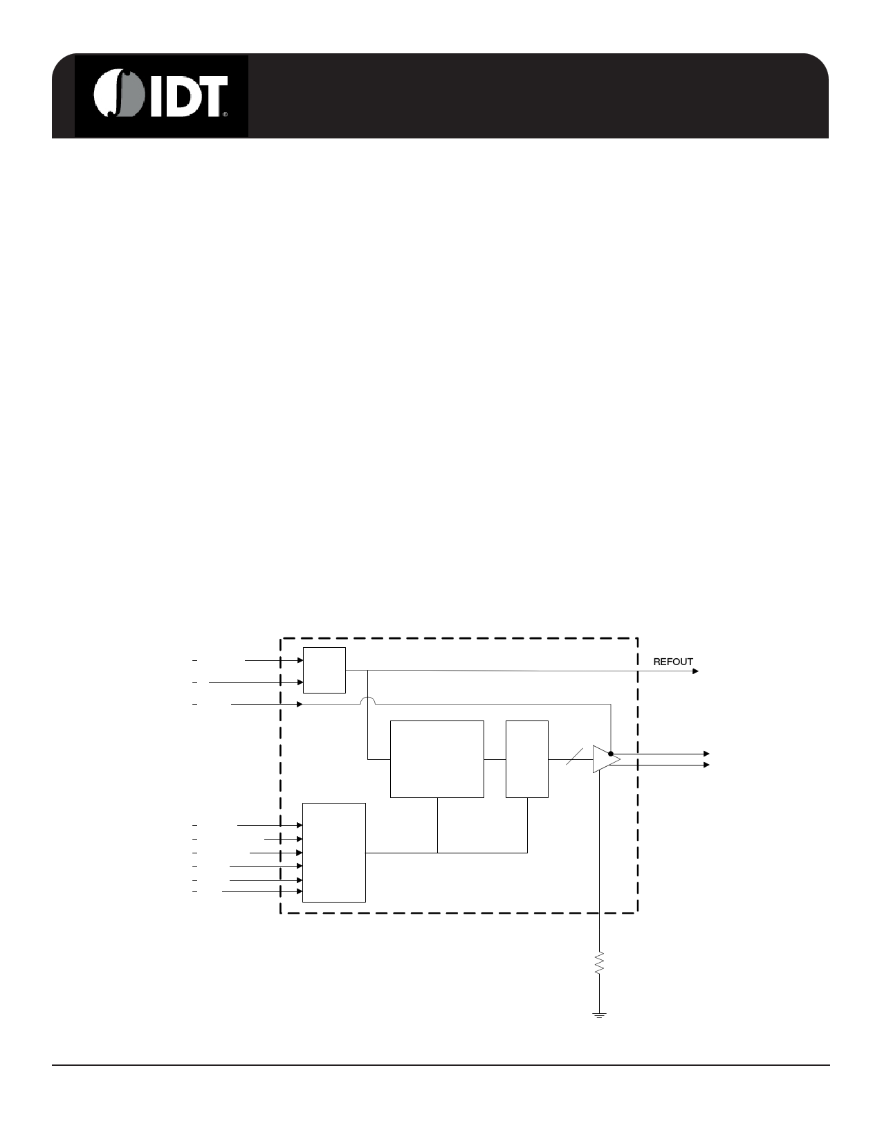
Functional Block Diagram
XIN/CLKIN
X2
OE(7:0)
OSC
PROGRAMMABLE
SPREAD PLL
STOP
LOGIC
8
REFOUT
DIF(7:0)
SPREAD
SEL14M_25M#
DIF_STOP#
FS(2:0)
SDATA
SCLK
CONTROL
LOGIC
IREF
IDT® Eight Output Differential Frequency Generator for PCIe Gen3 and QPI
1
1680C—08/26/10
1 page 
9FG830
Eight Output Differential Frequency Generator for PCIe Gen3 and QPI
Electrical Characteristics - Absolute Maximum Ratings
PARAMETER
SYMBOL
CONDITIONS
3.3V Core Supply Voltage VDDA
3.3V Logic Supply Voltage VDD
Input Low Voltage
VIL
Input High Voltage
VIH
Except for SMBus interface
Input High Voltage
VIHSMB
SMBus clock and data pins
Storage Temperature
Ts
Junction Temperature
Tj
Input ESD protection ESD prot
Human Body Model
1Guaranteed by design and characterization, not 100% tested in production.
2 Operation under these conditions is neither implied nor guaranteed.
MIN
GND-0.5
-65
2000
TYP
MAX
4.6
4.6
VDD+0.5V
5.5V
150
125
UNITS
V
V
V
V
V
°C
°C
V
NOTES
1,2
1,2
1
1
1
1
1
1
Electrical Characteristics - Input/Supply/Common Parameters
TA = TCOM or TIND; Supply Voltage VDD = 3.3 V +/-5%
PARAMETER
SYMBOL
CONDITIONS
MIN
TYP
MAX UNITS NOTES
Ambient Operating
Temperature
Input High Voltage
Input Low Voltage
TCOM
TIND
VIH
VIL
IIN
Commmercial range
Industrial range
Single-ended inputs, except SMBus, low
threshold and tri-level inputs
Single-ended inputs, except SMBus, low
threshold and tri-level inputs
Single-ended inputs, VIN = GND, VIN = VDD
0
-40
2
GND - 0.3
-5
70
85
VDD + 0.3
°C
°C
V
0.8 V
5 uA
Input Current
Single-ended inputs
IINP
VIN = 0 V; Inputs with internal pull-up resistors
-200
VIN = VDD; Inputs with internal pull-down resistors
200 uA
Input Frequency
Fin
SEL14M_25M# = 0
SEL14M_25M# = 1
Pin Inductance
Lpin
Capacitance
CIN
CINXTAL
Logic Inputs
Crystal inputs
COUT
Output pin capacitance
Clk Stabilization
TSTAB
From VDD Power-Up and after input clock
stabilization or de-assertion of PD# to 1st clock
SS Modulation Frequency fMODIN
Allowable Frequency
(Triangular Modulation)
OE# Latency
tLATOE#
DIF start after OE# assertion
DIF stop after OE# deassertion
Tdrive_STOP#
tDRVDS
DIF output enable after
DIF_STOP# de-assertion
Tfall tF Fall time of control inputs
Trise tR Rise time of control inputs
SMBus Input Low Voltage VILSMB
SMBus Input High Voltage VIHSMB
SMBus Output Low Voltage VOLSMB
@ IPULLUP
SMBus Sink Current
IPULLUP
@ VOL
Nominal Bus Voltage
VDDSMB
3V to 5V +/- 10%
SCLK/SDATA Rise Time
tRSMB
(Max VIL - 0.15) to (Min VIH + 0.15)
SCLK/SDATA Fall Time
SMBus Operating
Frequency
tFSMB
fMAXSMB
(Min VIH + 0.15) to (Max VIL - 0.15)
Maximum SMBus operating frequency
1Guaranteed by design and characterization, not 100% tested in production.
2Control input must be monotonic from 20% to 80% of input swing.
3Time from deassertion until outputs are >200 mV
25
14.31818
1.5
7
5
6
6
2.5
MHz
MHz
nH
pF
pF
pF
ms
30 33 kHz
1 3 cycles
300 us
5 ns
5 ns
0.8 V
2.1
VDDSMB
V
0.4 V
4 mA
2.7 5.5 V
1000
ns
300 ns
100 kHz
1
1
1
1
1
1
1
1
1
1
1
1
1,2
1
1,3
1,3
1,2
1,2
1
1
1
1
1
1
1
1
IDT® Eight Output Differential Frequency Generator for PCIe Gen3 and QPI
1680C—08/26/10
5
5 Page 
9FG830
Eight Output Differential Frequency Generator for PCIe Gen3 and QPI
Differential Clock Tolerances x1 - 14.31818MHz
Clock Periods - Differential Outputs with Spread Spectrum Disabled
SSC OFF
1 Clock
1us
Measurement Window
0.1s
0.1s
0.1s
or SSC +/- Synthesis
0.25%
Error
Center (ppm)
Spread
Center
Freq.
MHz
-c2c jitter
AbsPer
-SSC
Short-Term
Average
- ppm
Long-Term
Average
Min Min
Min
0 ppm
Period
Nominal
+ ppm
Long-Term
Average
Max
35 100.00 9.94965
-114 125.00 7.95091
35 133.33 7.44974
DIF
-104 166.67 5.95062
35 200.00 4.94983
42 266.67 3.69984
-104 333.33 2.95031
35 400.00 2.44991
9.99965
8.00091
7.49974
6.00062
4.99983
3.74984
3.00031
2.49991
10.00000
8.00000
7.50000
6.00000
5.00000
3.75000
3.00000
2.50000
10.00035
7.99909
7.50026
5.99937
5.00018
3.75016
2.99969
2.50009
1us
+SSC
Short-
Term
Average
Max
1 Clock
+c2c jitter Units
AbsPer
Max
10.05035
8.04909
7.55026
6.04937
5.05018
3.80016
3.04969
2.55009
ns
ns
ns
ns
ns
ns
ns
ns
Notes
1,2
1,2
1,2
1,2
1,2
1,2
1,2
1,2
Clock Periods - Differential Outputs with Spread Spectrum Enabled
Measurement Window
SSC ON
-0.5%
Down
Spread
Synthesis
Error
(ppm)
Center
Freq.
MHz
1 Clock
1us
0.1s
0.1s
0.1s
-c2c jitter
AbsPer
Min
-SSC
Short-Term
Average
Min
- ppm
Long-Term
Average
Min
0 ppm
Period
Nominal
+ ppm
Long-Term
Average
Max
199 99.75 9.94807 9.99807 10.02307 10.02506 10.02706
-100 124.69 7.95085 8.00085 8.02085 8.02005 8.01925
199 133.00 7.44855 7.49855 7.51730 7.51880 7.52029
DIF 10 166.25 5.94998 5.99998 6.01498 6.01504 6.01510
199 199.50 4.94903 4.99903 5.01153 5.01253 5.01353
-140 266.00 3.70055 3.75055 3.75992 3.75940 3.75887
10 332.50 2.94999 2.99999 3.00749 3.00752 3.00755
199 399.00 2.44952 2.49952 2.50577 2.50627 2.50676
1us 1 Clock
+SSC
Short- +c2c jitter Units
Term AbsPer
Average Max
Max
10.05206 10.10206 ns
8.03925 8.08925 ns
7.53904 7.58904 ns
6.03010 6.08010 ns
5.02603 5.07603 ns
3.76825 3.81825 ns
3.01505 3.06505 ns
2.51301 2.56301 ns
Notes
1,2
1,2
1,2
1,2
1,2
1,2
1,2
1,2
1Guaranteed by design and characterization, not 100% tested in production.
2 All Long Term Accuracy specifications are guaranteed with the assumption that the REF output is tuned to the exact target XTAL
frequency.
IDT® Eight Output Differential Frequency Generator for PCIe Gen3 and QPI
11
1680C—08/26/10
11 Page | ||
| Páginas | Total 19 Páginas | |
| PDF Descargar | [ Datasheet 9FG830.PDF ] | |
Hoja de datos destacado
| Número de pieza | Descripción | Fabricantes |
| 9FG830 | Eight Output Differential Frequency Generator | IDT |
| Número de pieza | Descripción | Fabricantes |
| SLA6805M | High Voltage 3 phase Motor Driver IC. |
Sanken |
| SDC1742 | 12- and 14-Bit Hybrid Synchro / Resolver-to-Digital Converters. |
Analog Devices |
|
DataSheet.es es una pagina web que funciona como un repositorio de manuales o hoja de datos de muchos de los productos más populares, |
| DataSheet.es | 2020 | Privacy Policy | Contacto | Buscar |