|
|
|
PDF MR37V12841A Data sheet ( Hoja de datos )
| Número de pieza | MR37V12841A | |
| Descripción | P2ROM | |
| Fabricantes | LAPIS | |
| Logotipo | ||
Hay una vista previa y un enlace de descarga de MR37V12841A (archivo pdf) en la parte inferior de esta página. Total 15 Páginas | ||
|
No Preview Available !
MR37V12841A
128M 1–Bit Serial Production Programmed ROM (P2ROM)
FEDR37V12841A-002-02
Issue Date: Oct. 01, 2008
GENERAL DESCRIPTION
The MR37V12841A is a 128Mbit Production Programmed Read-Only Memory, which is configured as
134,217,728word 1-bit. The MR37V12841A supports a simple read operation using a single 3.3V power supply
and a Serial Peripheral Interface (SPI) compatible serial bus.
The MR37V12841A have data programmed and have functions tested at LAPIS Semiconductor factory. (Using
the DC pins for the programming function is NOT allowed )
FEATURES
·Read Operation
- +3.3 V power supply
- 134,217,728 1-bit
- Access time: 33MHz serial clock (FAST-READ)
- 20MHz serial clock (READ)
- Read Identification Instruction
- Active read current: 30mA(FAST-READ)
- 20mA(READ)
- Standby current : 50 µA
- Serial Clock Input and Data Input/Output
- Input Data Format :
1-byte Command code, 3-byte address, 1-byte dummy
(FAST-READ)
1-byte Command code, 3-byte address
(READ)
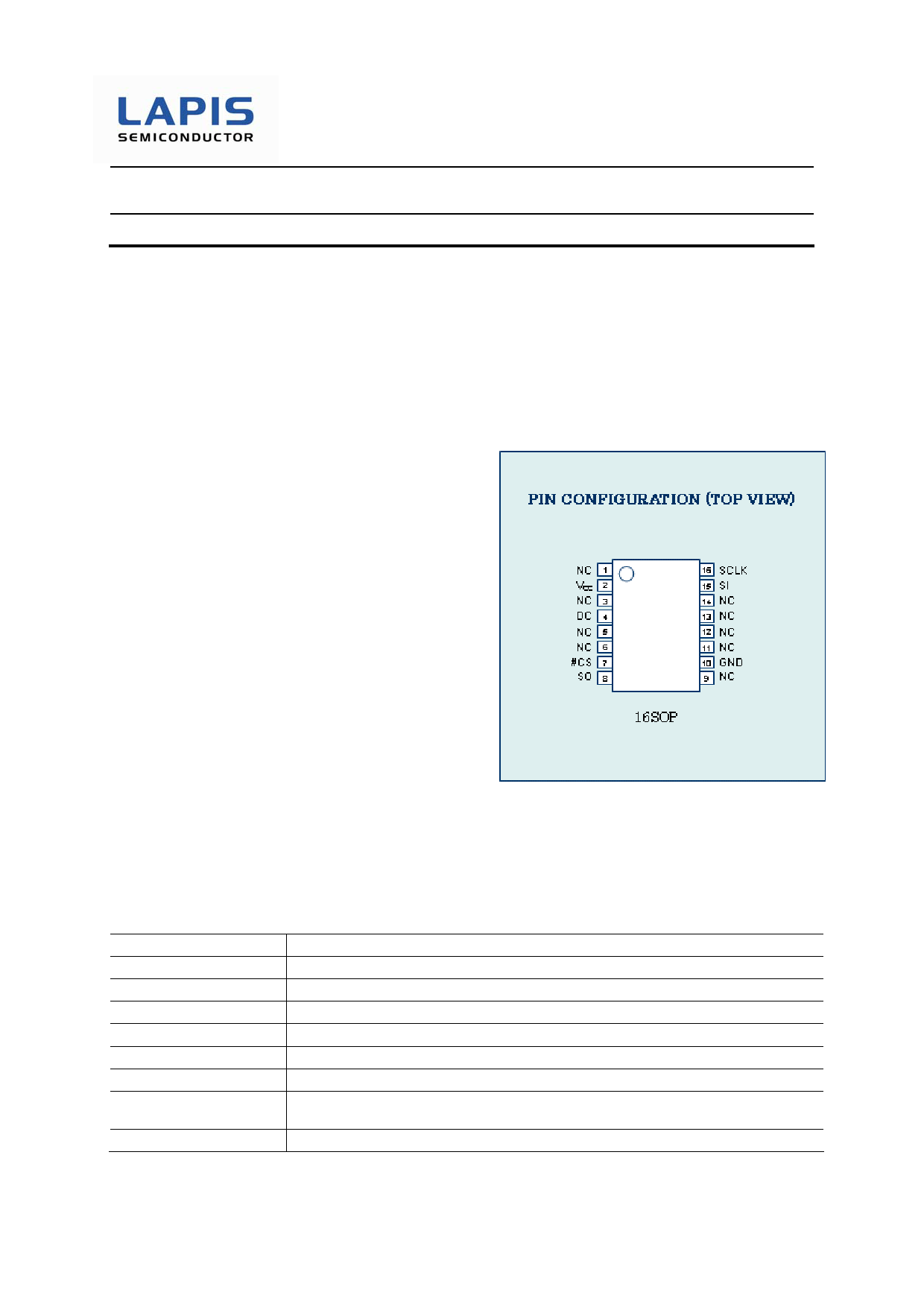
PACKAGES
· MR37V12841A-xxxMP
- 16-pin plastic SOP (P-SOP16-375-1.27-K)
PIN DESCRIPTIONS
Pin name
#CS
SI
SO
SCLK
VCC
GND
DC
NC
Functions under Read Operation
Chip Select
Serial Data Input
Serial Data Output
Clock Input
Power supply voltage
Ground
Don’t care ( 0v - Vcc )
<for reference> Program power supply voltage Vpp under Programming operation
Non connection
1/15
1 page 
FEDR37V12841A-002-02
MR37V12841A / P2ROM
DEVICE OPERATION
1. Command “03h” or “0Bh” makes this LSI become and keep active mode until next #CS High.
2. Incorrect command makes this LSI become and keep standby mode until next #CS Low. In standby mode, SO pin is
High-Z.
COMMAND DESCRIPTION
1. Read Array
This command consists of the 4-byte code. The 1st code is a command which decides if the device becomes standby
or active mode. The 1st code “03h” activates the device. The 2nd code to the 4th code are address inputs.
2. Fast Read Array
This command consists of the 5-byte code. The 1st code is a command which decides if the device becomes standby
or active mode. The 1st code “0Bh”activates the device. The 2nd code to the 4th code are address. The 5th code is a
dummy cycle.
3. Identification Read Array
This command consists of the 1-byte code. The 1st code is a command which decides if the device becomes standby
or active mode. The 1st code “9Fh”activates the device.
4. Standby
When #CS is high, the device is put in standby mode at the next rising edge of SCLK. Maximum standby current is
10uA. When the above-mentioned 1st code is incorrect command, the device is put in standby mode at the next rising
edge of SCLK.
DATA SEQUENCE
The data is serially sent out through SO pin, synchronized with the falling edge of SCLK. Meanwhile input data is also
serially read in through SI pin, synchronized with the rising edge of SCLK. The bit sequence for both input and output
data are bit7 (MSB) first, bit6, bit 5, …, and bit0(LSB).
ADDRESS SEQUENCE
The address assignment is described at the COMMAND DEFINITION on page 2, 3.
5/15
5 Page 
FEDR37V12841A-002-02
MR37V12841A / P2ROM
Fast Read Array Timing Waveform
#CS
SCLK
SI
SO
*note1
BIT 7 BIT 6 BIT 5 BIT 4 BIT 3 BIT 2 BIT 1 BIT 0 BIT 7 BIT 6 BIT 5 BIT 4 BIT 3
1st byte Command
2nd byte AD1
Hi-Z
#CS
SCLK
SI
SO
*note2
BIT 1 BIT 0
Don’t Care
5th byte DUMMY
Hi-Z
BIT 7 BIT 6 BIT 5 BIT 4 BIT 3 BIT 2 BIT 1 BIT 0 BIT 7 BIT 6 BIT 5
1st data output
2nd data output
#CS
SCLK
SI
SO BIT 3 BIT 2 BIT 1 BIT 0 BIT 7 BIT 6 BIT 5 BIT 4 BIT 3 BIT 2 BIT 1 BIT 0 BIT 7
Hi-Z
(N-1)th data output
Nth data output
(N+1)th data output
Note:
1. Input data are latched at SCLK-rising edge.
2. Data-output starts at SCLK-falling edge in bit0 of the 5th byte.
11/15
11 Page | ||
| Páginas | Total 15 Páginas | |
| PDF Descargar | [ Datasheet MR37V12841A.PDF ] | |
Hoja de datos destacado
| Número de pieza | Descripción | Fabricantes |
| MR37V12841A | P2ROM | LAPIS |
| Número de pieza | Descripción | Fabricantes |
| SLA6805M | High Voltage 3 phase Motor Driver IC. |
Sanken |
| SDC1742 | 12- and 14-Bit Hybrid Synchro / Resolver-to-Digital Converters. |
Analog Devices |
|
DataSheet.es es una pagina web que funciona como un repositorio de manuales o hoja de datos de muchos de los productos más populares, |
| DataSheet.es | 2020 | Privacy Policy | Contacto | Buscar |