|
|
|
PDF CY7C64215 Data sheet ( Hoja de datos )
| Número de pieza | CY7C64215 | |
| Descripción | enCoRe III Full-Speed USB Controller | |
| Fabricantes | Cypress Semiconductor | |
| Logotipo | ||
Hay una vista previa y un enlace de descarga de CY7C64215 (archivo pdf) en la parte inferior de esta página. Total 30 Páginas | ||
|
No Preview Available !
CY7C64215
enCoRe™ III Full-Speed USB Controller
enCoRe™ III Full-Speed USB Controller
Features
■ Powerful Harvard-architecture processor
❐ M8C processor speeds up to 24 MHz
❐ Two 8 × 8 multiply, 32-bit accumulate
❐ 3.15 to 5.25-V operating voltage
❐ USB 2.0 USB-IF certified. TID# 40000110
❐ Commercial operating temperature range: 0 °C to +70 °C
❐ Industrial operating temperature range: –40 °C to +85 °C
■ Advanced peripherals (enCoRe™ III blocks)
❐ Six analog enCoRe III blocks provide:
• Up to 14-bit incremental and delta sigma analog-to-digital
converters (ADCs)
❐ Programmable threshold comparator
❐ Four digital enCoRe III blocks provide:
• 8-bit and 16-bit pulse width modulators (PWMs), timers,
and counters
• I2C master
• SPI master or slave
• Full-duplex universal asynchronous receiver-transmitter
(UART)
• CYFISNP modules to talk to Cypress CYFI™ radio
■ Complex peripherals by combining blocks
■ Full-speed USB (12 Mbps)
❐ Four unidirectional endpoints
❐ One bidirectional control endpoint
❐ Dedicated 256-byte buffer
❐ No external crystal required
❐ Operational at 3.15 V to 3.5 V or 4.35 V to 5.25 V
■ Flexible on-chip memory
❐ 16 KB flash program storage 50,000 erase/write cycles
❐ 1 KB SRAM data storage
❐ In-system serial programming (ISSP)
❐ Partial flash updates
❐ Flexible protection modes
❐ EEPROM emulation in flash
■ Programmable pin configurations
❐ 25 mA sink on all general purpose I/Os (GPIOs)
❐ Pull-up, Pull-down, high Z, strong, or open drain drive modes
on all GPIOs
❐ Configurable interrupt on all GPIOs
■ Precision, programmable clocking
❐ Internal ±4% 24- and 48-MHz oscillator with support for
external clock oscillator
❐ Internal oscillator for watchdog and sleep
❐ .25% accuracy for USB with no external components
■ Additional system resources
❐ Inter-integrated circuit (I2C) slave, master, and multimaster
to 400 kHz
❐ Watchdog and sleep timers
❐ User-configurable low-voltage detection (LVD)
❐ Integrated supervisory circuit
❐ On-chip precision voltage reference
■ Complete development tools
❐ Free development software (PSoC® Designer)
❐ Full-featured, in-circuit emulator and programmer
❐ Full-speed emulation
❐ Complex breakpoint structure
❐ 128 KB trace memory
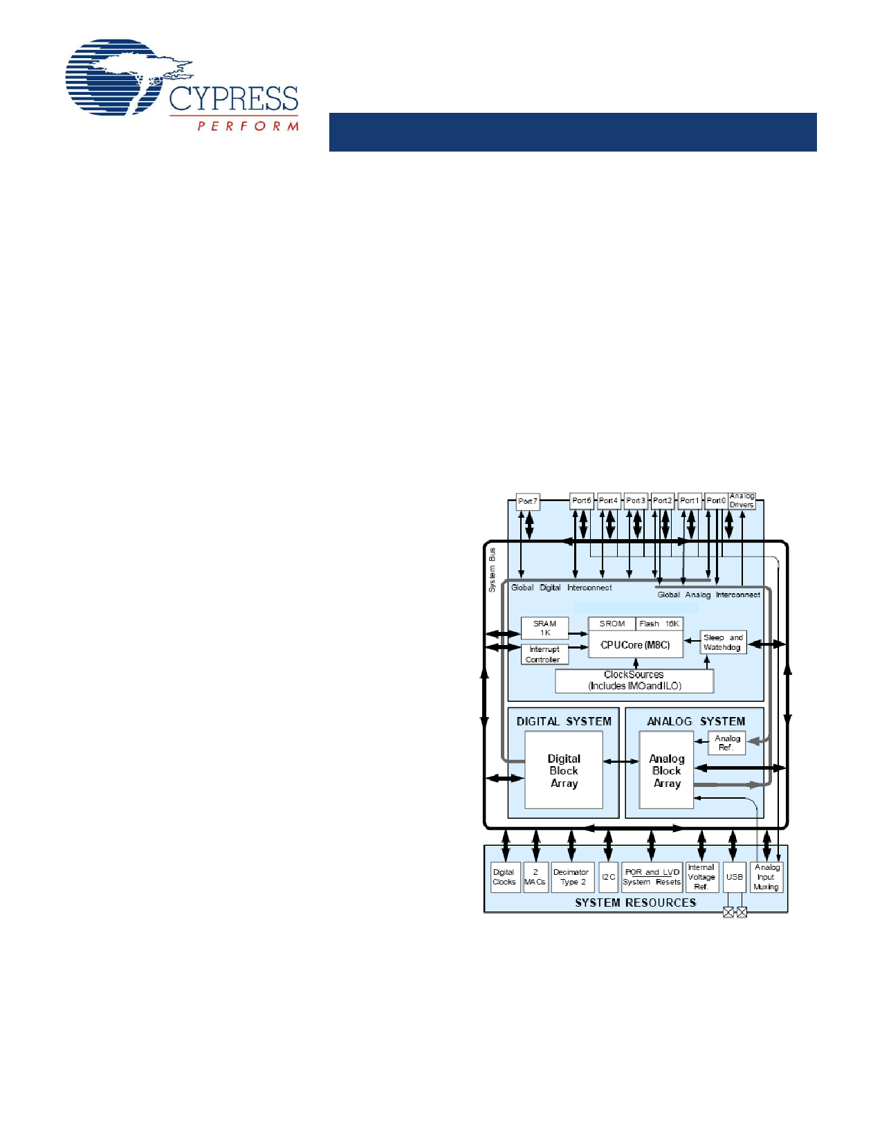
Block Diagram
enCoRe III Core
Errata: For information on silicon errata, see “Errata” on page 40. Details include trigger conditions, devices affected, and proposed workaround.
Cypress Semiconductor Corporation • 198 Champion Court
Document Number: 38-08036 Rev. *M
• San Jose, CA 95134-1709 • 408-943-2600
Revised August 28, 2014
1 page 
CY7C64215
Getting Started
The quickest path to understanding the enCoRe III silicon is by
reading this datasheet and using the PSoC Designer Integrated
Development Environment (IDE). This datasheet is an overview
of the enCoRe V integrated circuit and presents specific pin,
register, and electrical specifications.
For in-depth information, along with detailed programming
details, see the PSoC® Technical Reference Manual.
For up-to-date ordering, packaging, and electrical specification
information, see the latest PSoC device datasheets on the web.
Application Notes
Cypress application notes are an excellent introduction to the
wide variety of possible PSoC designs.
Development Kits
PSoC Development Kits are available online from and through a
growing number of regional and global distributors, which
include Arrow, Avnet, Digi-Key, Farnell, Future Electronics, and
Newark.
Training
Free PSoC technical training (on demand, webinars, and
workshops), which is available online via www.cypress.com,
covers a wide variety of topics and skill levels to assist you in
your designs.
CYPros Consultants
Certified PSoC consultants offer everything from technical
assistance to completed PSoC designs. To contact or become a
PSoC consultant go to the CYPros Consultants web site.
Solutions Library
Visit our growing library of solution focused designs. Here you
can find various application designs that include firmware and
hardware design files that enable you to complete your designs
quickly.
Technical Support
Technical support – including a searchable Knowledge Base
articles and technical forums – is also available online. If you
cannot find an answer to your question, call our Technical
Support hotline at 1-800-541-4736.
Development Tools
PSoC Designer™ is the revolutionary integrated design
environment (IDE) that you can use to customize PSoC to meet
your specific application requirements. PSoC Designer software
accelerates system design and time to market. Develop your
applications using a library of precharacterized analog and digital
peripherals (called user modules) in a drag-and-drop design
environment. Then, customize your design by leveraging the
dynamically generated application programming interface (API)
libraries of code. Finally, debug and test your designs with the
integrated debug environment, including in-circuit emulation and
standard software debug features. PSoC Designer includes:
■ Application editor graphical user interface (GUI) for device and
user module configuration and dynamic reconfiguration
■ Extensive user module catalog
■ Integrated source-code editor (C and assembly)
■ Free C compiler with no size restrictions or time limits
■ Built-in debugger
■ In-circuit emulation
■ Built-in support for communication interfaces:
❐ Hardware and software I2C slaves and masters
❐ Full-speed USB 2.0
❐ Up to four full-duplex universal asynchronous
receiver/transmitters (UARTs), SPI master and slave, and
wireless
PSoC Designer supports the entire library of PSoC 1 devices and
runs on Windows XP, Windows Vista, and Windows 7.
PSoC Designer Software Subsystems
Design Entry
In the chip-level view, choose a base device to work with. Then
select different onboard analog and digital components that use
the PSoC blocks, which are called user modules. Examples of
user modules are ADCs, DACs, amplifiers, and filters. Configure
the user modules for your chosen application and connect them
to each other and to the proper pins. Then generate your project.
This prepopulates your project with APIs and libraries that you
can use to program your application.
The tool also supports easy development of multiple
configurations and dynamic reconfiguration. Dynamic
reconfiguration makes it possible to change configurations at run
time. In essence, this allows you to use more than 100 percent
of PSoC’s resources for an application.
Code Generation Tools
The code generation tools work seamlessly within the
PSoC Designer interface and have been tested with a full range
of debugging tools. You can develop your design in C, assembly,
or a combination of the two.
Assemblers. The assemblers allow you to merge assembly
code seamlessly with C code. Link libraries automatically use
absolute addressing or are compiled in relative mode, and are
linked with other software modules to get absolute addressing.
C Language Compilers. C language compilers are available
that support the PSoC family of devices. The products allow you
to create complete C programs for the PSoC family devices. The
optimizing C compilers provide all of the features of C, tailored
to the PSoC architecture. They come complete with embedded
libraries providing port and bus operations, standard keypad and
display support, and extended math functionality.
Debugger
PSoC Designer has a debug environment that provides
hardware in-circuit emulation, allowing you to test the program in
a physical system while providing an internal view of the PSoC
device. Debugger commands allow you to read and program and
read and write data memory, and read and write I/O registers.
You can read and write CPU registers, set and clear breakpoints,
Document Number: 38-08036 Rev. *M
Page 5 of 45
5 Page 
CY7C64215
Register Map Bank 1 Table: Configuration Space
Name
PRT0DM0
Addr
(1,Hex)
Access
00 RW
Name
PMA0_WA
Addr
(1,Hex)
40
Access
RW
PRT0DM1
01
RW
PMA1_WA 41 RW
PRT0IC0 02 RW
PMA2_WA 42 RW
PRT0IC1 03 RW
PMA3_WA 43 RW
PRT1DM0
04
RW
PMA4_WA 44 RW
PRT1DM1
05
RW
PMA5_WA 45 RW
PRT1IC0 06 RW
PMA6_WA 46 RW
PRT1IC1 07 RW
PMA7_WA 47 RW
PRT2DM0
08
RW
48
PRT2DM1
09
RW
49
PRT2IC0 0A RW
4A
PRT2IC1 0B RW
4B
PRT3DM0
0C
RW
4C
PRT3DM1
0D
RW
4D
PRT3IC0 0E RW
4E
PRT3IC1 0F RW
4F
PRT4DM0
10
RW
PMA0_RA
50 RW
PRT4DM1
11
RW
PMA1_RA
51 RW
PRT4IC0 12 RW
PMA2_RA
52 RW
PRT4IC1 13 RW
PMA3_RA
53 RW
PRT5DM0
14
RW
PMA4_RA
54 RW
PRT5DM1
15
RW
PMA5_RA
55 RW
PRT5IC0 16 RW
PMA6_RA
56 RW
PRT5IC1 17 RW
PMA7_RA
57 RW
18 58
19 59
1A 5A
1B 5B
PRT7DM0
1C
RW
5C
PRT7DM1
1D
RW
5D
PRT7IC0 1E RW
5E
PRT7IC1 1F RW
5F
DBB00FN
20
RW
CLK_CR0
60 RW
DBB00IN 21 RW
CLK_CR1
61 RW
DBB00OU
22
RW
ABF_CR0
62 RW
23
AMD_CR0
63 RW
DBB01FN
24
RW
CMP_GO_EN
64
RW
DBB01IN 25 RW
65 RW
DBB01OU
26
RW
AMD_CR1
66 RW
27
ALT_CR0
67 RW
DCB02FN
28
RW
68
DCB02IN 29 RW
69
DCB02OU
2A
RW
6A
2B 6B
DCB03FN
2C
RW
TMP_DR0
6C RW
DCB03IN 2D RW
TMP_DR1
6D RW
DCB03OU
2E
RW
TMP_DR2
6E RW
2F
TMP_DR3
6F RW
30
ACB00CR3
70
RW
31
ACB00CR0
71
RW
32
ACB00CR1
72
RW
33
ACB00CR2
73
RW
34
ACB01CR3
74
RW
35
ACB01CR0
75
RW
36
ACB01CR1
76
RW
37
ACB01CR2
77
RW
38 78
39 79
3A 7A
3B 7B
3C 7C
3D 7D
3E 7E
3F 7F
Blank fields are Reserved and should not be accessed.
Name
ASC10CR0
Addr
(1,Hex)
80
ASC10CR1
81
ASC10CR2
82
ASC10CR3
83
ASD11CR0
84
ASD11CR1
85
ASD11CR2
86
ASD11CR3
87
88
89
8A
8B
8C
8D
8E
8F
90
ASD20CR1
91
ASD20CR2
92
ASD20CR3
93
ASC21CR0
94
ASC21CR1
95
ASC21CR2
96
ASC21CR3
97
98
99
9A
9B
9C
9D
9E
9F
A0
A1
A2
A3
A4
A5
A6
A7
A8
A9
AA
AB
AC
AD
AE
AF
RDI0RI
B0
RDI0SYN
B1
RDI0IS
B2
RDI0LT0
B3
RDI0LT1
B4
RDI0RO0
B5
RDI0RO1
B6
B7
B8
B9
BA
BB
BC
BD
BE
BF
# Access is bit specific.
Access
RW
RW
RW
RW
RW
RW
RW
RW
RW
RW
RW
RW
RW
RW
RW
RW
RW
RW
RW
RW
RW
RW
Name
USBIO_CR2
USB_CR1
EP1_CR0
EP2_CR0
EP3_CR0
EP4_CR0
GDI_O_IN
GDI_E_IN
GDI_O_OU
GDI_E_OU
MUX_CR0
MUX_CR1
MUX_CR2
MUX_CR3
OSC_GO_EN
OSC_CR4
OSC_CR3
OSC_CR0
OSC_CR1
OSC_CR2
VLT_CR
VLT_CMP
IMO_TR
ILO_TR
BDG_TR
ECO_TR
MUX_CR4
MUX_CR5
CPU_F
DAC_CR
CPU_SCR1
CPU_SCR0
Addr
(1,Hex)
C0
C1
Access
RW
#
C4 #
C5 #
C6 #
C7 #
C8
C9
CA
CB
CC
CD
CE
CF
D0 RW
D1 RW
D2 RW
D3 RW
D4
D5
D6
D7
D8 RW
D9 RW
DA RW
DB RW
DC
DD RW
DE RW
DF RW
E0 RW
E1 RW
E2 RW
E3 RW
E4 R
E5
E6
E7
E8 W
E9 W
EA RW
EB W
EC RW
ED RW
EE
EF
F0
F1
F2
F3
F4
F5
F6
F7 RL
F8
F9
FA
FB
FC
FD RW
FE #
FF #
Document Number: 38-08036 Rev. *M
Page 11 of 45
11 Page | ||
| Páginas | Total 30 Páginas | |
| PDF Descargar | [ Datasheet CY7C64215.PDF ] | |
Hoja de datos destacado
| Número de pieza | Descripción | Fabricantes |
| CY7C64215 | enCoRe III Full-Speed USB Controller | Cypress Semiconductor |
| Número de pieza | Descripción | Fabricantes |
| SLA6805M | High Voltage 3 phase Motor Driver IC. |
Sanken |
| SDC1742 | 12- and 14-Bit Hybrid Synchro / Resolver-to-Digital Converters. |
Analog Devices |
|
DataSheet.es es una pagina web que funciona como un repositorio de manuales o hoja de datos de muchos de los productos más populares, |
| DataSheet.es | 2020 | Privacy Policy | Contacto | Buscar |