|
|
|
PDF AD9628 Data sheet ( Hoja de datos )
| Número de pieza | AD9628 | |
| Descripción | Dual Analog-to-Digital Converter | |
| Fabricantes | Analog Devices | |
| Logotipo | ||
Hay una vista previa y un enlace de descarga de AD9628 (archivo pdf) en la parte inferior de esta página. Total 30 Páginas | ||
|
No Preview Available !
Data Sheet
12-Bit, 125/105 MSPS, 1.8 V Dual
Analog-to-Digital Converter
AD9628
FEATURES
1.8 V analog supply operation
1.8 V CMOS or LVDS outputs
SNR = 71.2 dBFS @ 70 MHz
SFDR = 93 dBc @ 70 MHz
Low power: 101 mW/channel @ 125 MSPS
Differential analog input with 650 MHz bandwidth
IF sampling frequencies to 200 MHz
On-chip voltage reference and sample-and-hold circuit
2 V p-p differential analog input
DNL = ±0.25 LSB
Serial port control options
Offset binary, Gray code, or twos complement data format
Optional clock duty cycle stabilizer
Integer 1-to-8 input clock divider
Data output multiplex option
Built-in selectable digital test pattern generation
Energy-saving power-down modes
Data clock out with programmable clock and data
alignment
APPLICATIONS
Communications
Diversity radio systems
Multimode digital receivers
GSM, EDGE, W-CDMA, LTE,
CDMA2000, WiMAX, TD-SCDMA
I/Q demodulation systems
Smart antenna systems
Broadband data applications
Battery-powered instruments
Hand-held scope meters
Portable medical imaging
Ultrasound
Radar/LIDAR
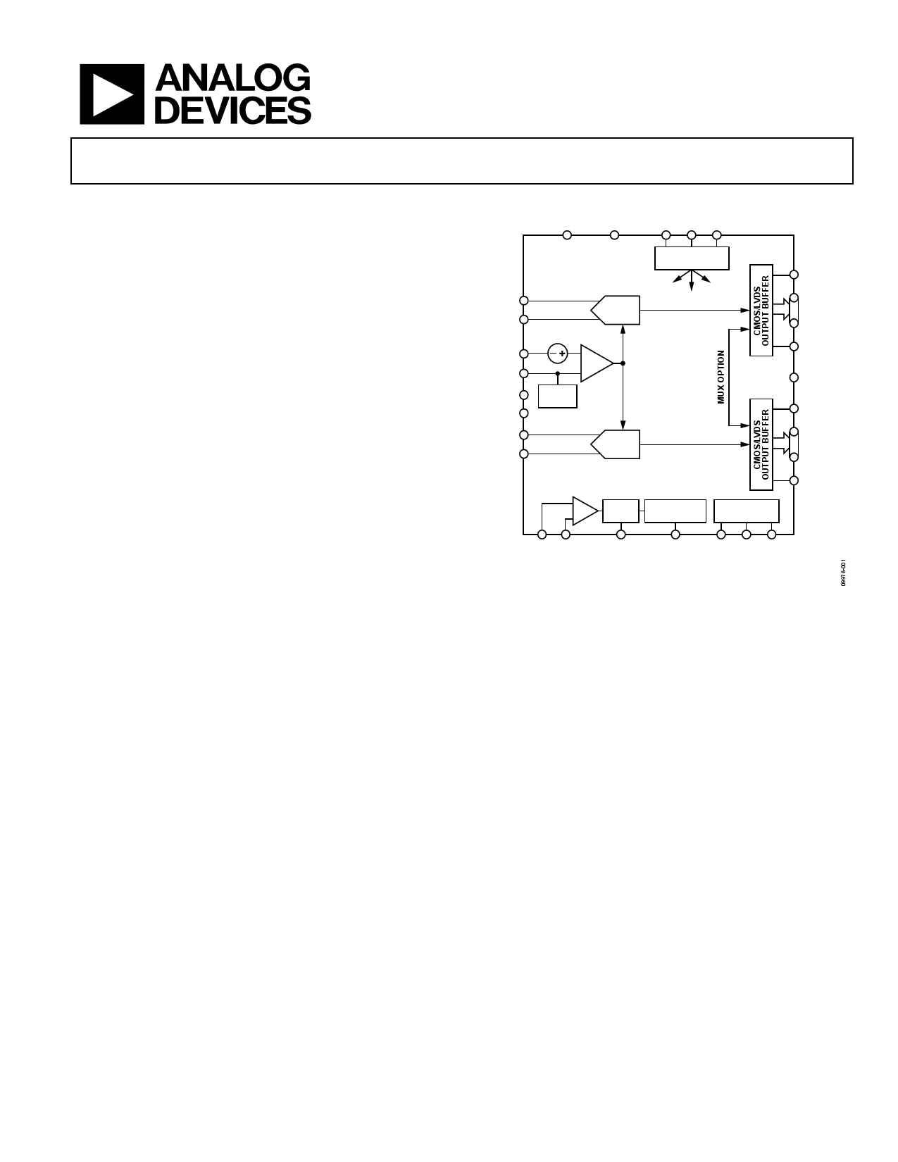
FUNCTIONAL BLOCK DIAGRAM
AVDD
AGND
SDIO SCLK CSB
VIN+A
VIN–A
VREF
SENSE
VCM
RBIAS
VIN–B
VIN+B
REF
SELECT
SPI
ADC
PROGRAMMING DATA
AD9628
ADC
DIVIDE DUTY CYCLE
1 TO 8 STABILIZER
MODE
CONTROLS
ORA
D11A
D0A
DCOA
DRVDD
ORB
D11B
D0B
DCOB
CLK+ CLK–
SYNC
DCS
PDWN DFS OEB
NOTES
1. PIN NAMES ARE FOR THE CMOS PIN CONFIGURATION ONLY;
SEE FIGURE 7 FOR LVDS PIN NAMES.
Figure 1.
PRODUCT HIGHLIGHTS
1. The AD9628 operates from a single 1.8 V analog power
supply and features a separate digital output driver supply
to accommodate 1.8 V CMOS or LVDS logic families.
2. The patented sample-and-hold circuit maintains excellent
performance for input frequencies up to 200 MHz and is
designed for low cost, low power, and ease of use.
3. A standard serial port interface supports various product
features and functions, such as data output formatting,
internal clock divider, power-down, DCO/data timing and
offset adjustments.
4. The AD9628 is packaged in a 64-lead RoHS-compliant
LFCSP that is pin compatible with the AD9650/AD9269/
AD9268 16-bit ADC, the AD9258/AD9251/AD9648 14-bit
ADCs, the AD9231 12-bit ADC, and the AD9608/AD9204
10-bit ADCs, enabling a simple migration path between
10-bit and 16-bit converters sampling from 20 MSPS to
125 MSPS.
Rev. C
Document Feedback
Information furnished by Analog Devices is believed to be accurate and reliable. However, no
responsibilityisassumedbyAnalogDevices for itsuse,nor foranyinfringementsofpatentsor other
rights of third parties that may result from its use. Specifications subject to change without notice. No
license is granted by implication or otherwise under any patent or patent rights of Analog Devices.
Trademarksandregisteredtrademarksarethepropertyoftheirrespectiveowners.
One Technology Way, P.O. Box 9106, Norwood, MA 02062-9106, U.S.A.
Tel: 781.329.4700 ©2011–2015 Analog Devices, Inc. All rights reserved.
Technical Support
www.analog.com
1 page 
Data Sheet
AD9628
Parameter
POWER CONSUMPTION
DC Input
Sine Wave Input (DRVDD = 1.8 V CMOS
Output Mode)1
Sine Wave Input (DRVDD = 1.8 V LVDS
Output Mode)1
Standby Power3
Power-Down Power
AD9628-105
Temp Min Typ
Max
Full 129
Full 173 182
Full 243
Full 108
Full 2.0
Min
1 Measured with a low input frequency, full-scale sine wave, with approximately 5 pF loading on each output bit.
2 Input capacitance refers to the effective capacitance between one differential input pin and AGND.
3 Standby power is measured with a dc input and with the CLK± pins active (1.8 V CMOS mode).
AD9628-125
Typ Max
148
201 212
269
120
2.0
Unit
mW
mW
mW
mW
mW
AC SPECIFICATIONS
AVDD = 1.8 V, DRVDD = 1.8 V, maximum sample rate, VIN = −1.0 dBFS differential input, 1.0 V internal reference, DCS enabled, unless
otherwise noted.
Table 2.
Parameter1
SIGNAL-TO-NOISE-RATIO (SNR)
fIN = 9.7 MHz
fIN = 30.5 MHz
fIN = 70 MHz
fIN = 100 MHz
fIN = 200 MHz
SIGNAL-TO-NOISE AND DISTORTION (SINAD)
fIN = 9.7 MHz
fIN = 30.5 MHz
fIN = 70 MHz
fIN = 100 MHz
fIN = 200 MHz
EFFECTIVE NUMBER OF BITS (ENOB)
fIN = 9.7 MHz
fIN = 30.5 MHz
fIN = 70 MHz
fIN = 100 MHz
fIN = 200 MHz
WORST SECOND OR THIRD HARMONIC
fIN = 9.7 MHz
fIN = 30.5 MHz
fIN = 70 MHz
fIN = 100 MHz
fIN = 200 MHz
Temp
25°C
25°C
25°C
Full
25°C
25°C
25°C
25°C
25°C
Full
25°C
25°C
25°C
25°C
25°C
25°C
25°C
25°C
25°C
25°C
Full
25°C
25°C
Min
70.6
70.5
AD9628-105
Typ Max
71.6
71.6
71.3
71.0
69.4
71.5
71.5
71.2
69.9
68.1
11.6
11.6
11.6
11.5
11.0
−92
−90
−90
−82
−89
−83
AD9628-125
Min Typ Max
71.5
71.4
71.2
70.2
70.9
69.6
71.4
71.3
71.1
70
69.8
68.3
11.6
11.6
11.5
11.3
11.1
−92
−90
−93
−85
−90
−84
Unit
dBFS
dBFS
dBFS
dBFS
dBFS
dBFS
dBFS
dBFS
dBFS
dBFS
dBFS
dBFS
Bits
Bits
Bits
Bits
Bits
dBc
dBc
dBc
dBc
dBc
dBc
Rev. C | Page 5 of 42
5 Page 
Data Sheet
CLK+
SYNC
tSSYNC
tHSYNC
Figure 5. SYNC Input Timing Requirements
AD9628
Rev. C | Page 11 of 42
11 Page | ||
| Páginas | Total 30 Páginas | |
| PDF Descargar | [ Datasheet AD9628.PDF ] | |
Hoja de datos destacado
| Número de pieza | Descripción | Fabricantes |
| AD9620 | Ultralow Distortion Buffer | Analog Devices |
| AD9621 | Wideband Voltage Feedback Amplifier | Analog Devices |
| AD9622 | Wideband Voltage Feedback Amplifier | Analog Devices |
| AD9623 | Wideband Voltage Feedback Amplifier | Analog Devices |
| Número de pieza | Descripción | Fabricantes |
| SLA6805M | High Voltage 3 phase Motor Driver IC. |
Sanken |
| SDC1742 | 12- and 14-Bit Hybrid Synchro / Resolver-to-Digital Converters. |
Analog Devices |
|
DataSheet.es es una pagina web que funciona como un repositorio de manuales o hoja de datos de muchos de los productos más populares, |
| DataSheet.es | 2020 | Privacy Policy | Contacto | Buscar |